Double-sided PCB

Double-sided PCBs feature conductive copper on both sides, allowing for more complex circuit designs compared to single-sided boards. This design is ideal for compact electronics, enabling component placement on both sides to maximize functionality. Vias, small holes plated with copper, connect the layers and facilitate intricate circuit layouts. Double-sided PCBs balance the simplicity and cost-effectiveness of single-sided boards with the high density of multilayer options, making them suitable for a variety of applications, including consumer electronics and power supplies.

Double-sided PCB Stackup

Typical laminate used for DSB

Typical substrates used for double-Sided board are CEM-3 and FR-4. 

CEM-3

Features a nonwoven fiberglass core with woven fiberglass cloth surfaces, impregnated with epoxy resin. Allows for plated-through holes. Often found in home computers, automobiles, and home entertainment products.

Most widely used material, made from woven fiberglass cloth impregnated with epoxy resin or its blend. Offers excellent electrical, mechanical, and thermal properties. Suitable for demanding applications like computers, telecommunications, aerospace, industrial controls, and automotive systems.

PTH & Via

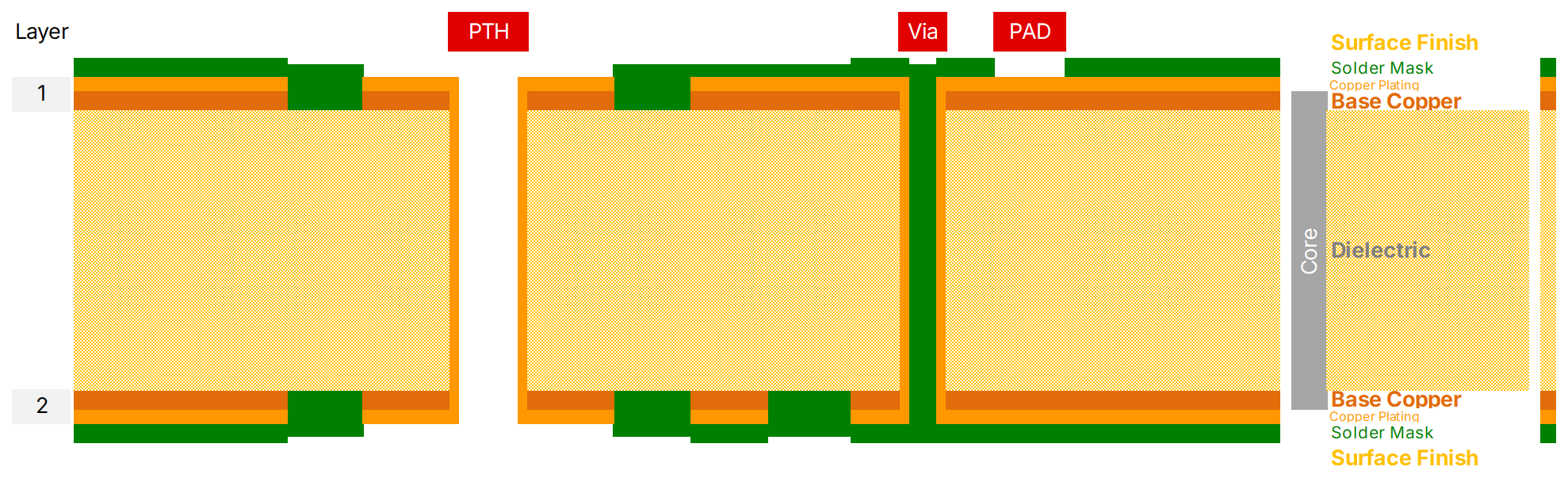
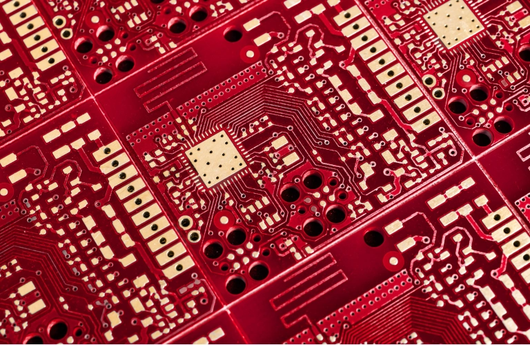
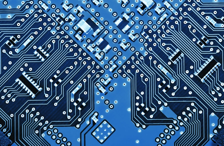
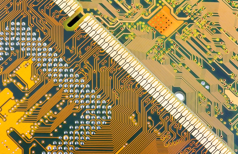
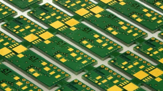
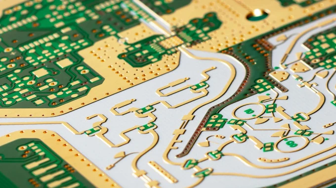
PTH(Plated-through-hole) technology is used in printed wiring boards (PWBs) to create electrical connections between different layers by metallizing the holes drilled through the boards. This method has been in practice since the mid-1950s and has undergone significant advancements over the decades.

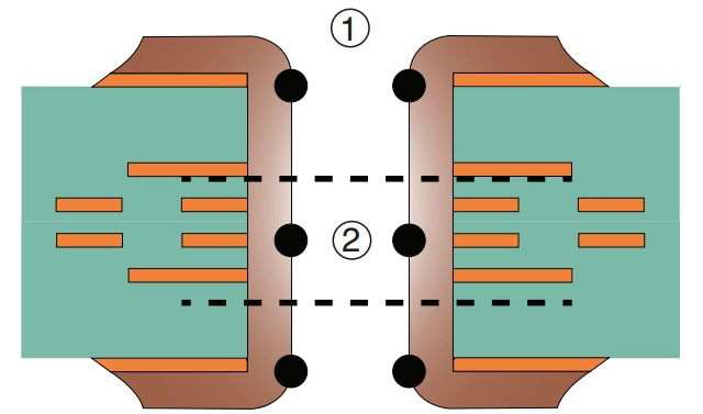
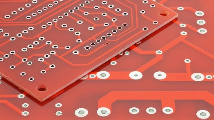
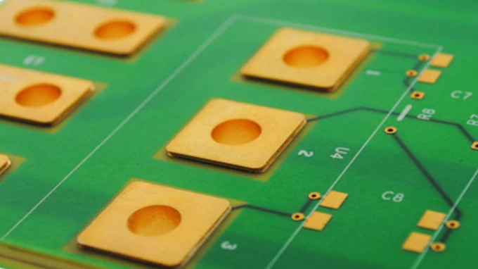
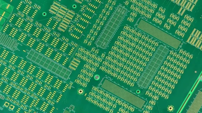
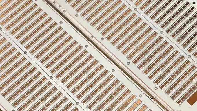
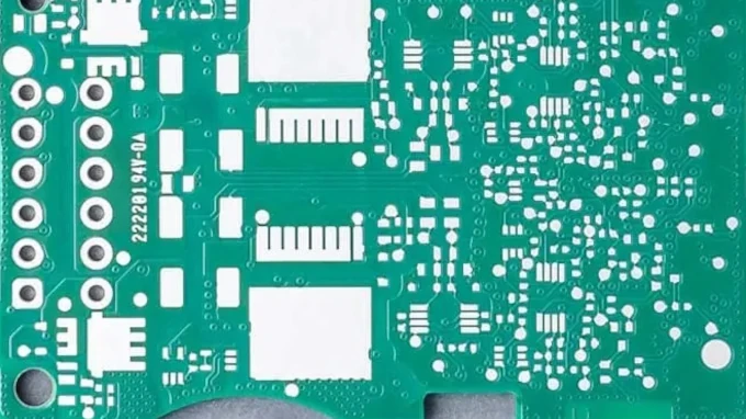
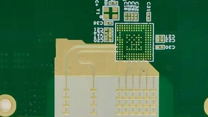
Via is a plated-through hole that connects different layers of a multilayer board, enabling electrical signals to pass between layers. Types include through-hole, blind, and buried vias. They can also be filled or capped for added reliability. The quality and reliability of vias are critical, as defects can cause board failures, especially in high-density or mission-critical applications. Standards like IPC-4761 provide guidelines for via design and protection.

Hole Copper Plating

Hole copper plating thicknesses shall meet the requirements of Table 3-10 through Table 3-12, shall be continuous and shall extend or wrap from hole walls onto outer surfaces (Refer to IPC-A-600 for discussion on copper plating thickness for hol walls). Deviations to these requirements shall be AABUS. Each side of the plated hole wall shall be evaluated independently. Measurements of the plating thickness shall be reported as an average thickness of 3 measurements per side of the hole. At least one measurement shall be taken within 40 – 60% of the hole height. Isolated thick or thin sections shall not be used for averaging. Isolated areas of reduced copper thickness due to glass fiber protrusions shall meet the minimum thickness requirements of Table 3-10 through Table 3-12 as measured from the end of the protrusion to the hole wall.

Minimum Internal Layer Copper Foil Thickness

If the internal conductor thickness of the finished printed board is specified by a foil weight, the minimum internal copper foil thickness after processing shall be measured in accordance with Table 3-17 for all classes. When the procurement documentation specifies a minimum copper thickness, the conductor shall meet or exceed that minimum thickness.

The requirements in Table 3-17 are based on minimum copper foil thickness allowances per IPC-4562 followed by two successive scrubbings. Each scrub is expected to remove a specific amount of copper and is represented by a variable processing allowance reduction.

Minimum Surface Conductor Thickness

If the internal conductor thickness of the finished printed board is specified by a foil weight, the minimum internal copper foil thickness after processing shall be measured in accordance with Table 3-17 for all classes. When the procurement documentation specifies a minimum copper thickness, the conductor shall meet or exceed that minimum thickness.

The requirements in Table 3-17 are based on minimum copper foil thickness allowances per IPC-4562 followed by two successive scrubbings. Each scrub is expected to remove a specific amount of copper and is represented by a variable processing allowance reduction.

PCB Soldermask

Soldermask is a thin protective coating applied to the surface of a PCB to insulate copper traces from environmental factors and prevent accidental solder bridges during component soldering. It is usually green but can come in other colors and plays a crucial role in enhancing PCB durability, reliability, and manufacturability by preventing short circuits and corrosion. Soldermask key functions:

1. Prevents Solder Bridging

Soldermask masks off and insulates the non-pad copper areas, preventing accidental solder bridges between adjacent pads or traces during soldering.

It shields the copper from oxidation, dust, moisture, and contaminants, enhancing the PCB’s durability and reliability over time.

Provides electrical insulation between conductors and protects the surface from physical damage and environmental stress.

Improves solder wetting and solder joint quality by clearly defining where solder should be deposited.

Surface Finish

Most PCBs use copper as their primary conductor. If the copper is left unprotected after finishing, it can oxidize, making soldering difficult. An ideal surface finish would possess good solderability, a flat coplanar surface, cost-effectiveness, the ability to withstand unlimited heat cycles, and minimal health and safety concerns. There are various final finishes available, each with its own advantages and disadvantages. Different finishes are more suitable for specific applications.

OSP(Organic Solderability Preservatives)

OSP is exceptionally thin organic coatings specifically formulated to preserve the solderability of copper surfaces on PCB. This coating works by forming a complex organo-metallic bond with the copper, which is critical for ensuring a reliable solderable finish. OSP is particularly suitable for a range of applications, including both surface mount and through-hole assembly processes. Additionally, they offer a shelf life that supports effective long-term storage without compromising solderability, making them a practical choice for manufacturers and engineers alike.

Hot Air Solder Level (HASL or HAL) is the process of immersing a circuit board into molten solder, immediately followed by blowing the excess molten solder out of the holes using hot air under high pressure. For the vast majority of HASL applications, the solder alloy is tin-lead. For Pb-free applications, the main alloys include tin-copper, tin-silver-copper, tin-copper-nickel, and tin-copper-nickel-germanium alloys.

Other types of Double-sided PCBs

In addition to standard FR-4, double-sided PCBs include metal-core (MCPCB) for high-power LED/automotive applications, flexible PCBs for bendable electronics, and high-frequency laminates (like Rogers) for RF/microwave circuits etc. These offer superior thermal management, flexibility, or signal integrity for specialized designs.

Double-sided Aluminum-Based PCBs

Double-sided aluminum-based PCBs are printed circuit boards featuring two conductive copper layers on either side of an electrically insulating dielectric, which is itself bonded to an aluminum base. This structure allows for complex circuitry and component mounting on both sides of the board, enhancing design flexibility and circuit density. The aluminum core offers excellent heat dissipation, making these PCBs ideal for applications with high power or thermal demands, such as LED lighting, automotive, and power electronics. They also provide improved mechanical durability and better EMI shielding compared to standard FR4 boards.

Double-sided Copper-Based PCBs

Double-sided copper-based PCBs are printed circuit boards featuring conductive copper layers on both sides, bonded to a thermally conductive substrate, typically aluminum or copper. These boards excel in heat dissipation, making them ideal for high-power applications like LED lighting, power supplies, and automotive electronics. The dual copper layers allow for more complex circuit designs and higher component density compared to single-sided versions. Vias (plated-through holes) enable electrical connections between layers, enhancing functionality. Their robust thermal management ensures reliability in demanding environments. Double-sided copper PCBs offer a balance of performance, durability, and design flexibility, catering to advanced electronic and industrial applications.

Double-sided FPC

Double-sided flexible printed circuit boards (PCBs) are composed of two conductive layers separated by a flexible insulating substrate, allowing for circuit traces on both sides. These PCBs enable more complex designs compared to single-sided versions and can incorporate plated through-holes, enabling electrical connections between the two sides. Their flexibility makes them ideal for applications requiring dynamic bending or where space and weight constraints are critical, such as in medical devices, wearable electronics, and aerospace equipment. Overall, double-sided flexible PCBs offer improved design versatility, increased circuit density, and reliable performance in challenging mechanical environments.

What information is required for double-sided PCB fabrication?

Essential information includes part numbers, fabrication and drill drawings, manufacturing notes, board details, material specifications, conductor patterns, artwork data for both sides, aperture lists, drill data, netlist data, and any special requirements.

Designers must plan via placement carefully, optimize trace width/spacing for signal integrity, and ensure thermal relief around plated through-holes for reliable soldering and heat dissipation.

Common substrates include glass fiber (like FR-4) combined with epoxy resin, and copper is used for both top and bottom conductive traces, often specified by weight (e.g., 1 oz or 0.5 oz copper).

The process includes drilling holes through the board, plating copper inside the holes to create electrical connections, etching traces on both sides, applying solder mask, and adding surface finishes like HASL or ENIG.

Quality control includes electrical testing, comparison of netlists, automated optical inspection (AOI), and conformity with IPC standards to ensure the finished PCB matches the intended design and performance criteria.

Are double-sided PCBs more expensive than single-sided PCBs?

Yes, due to the additional plating, drilling, and assembly steps. However, they reduce overall system size and component costs, often justifying the added expense.

They are used in automotive electronics, LED lighting systems, power supplies, industrial control units, consumer electronics, and telecommunication devices.

They enable higher circuit density, support more components, reduce board size, and allow designers to route complex circuits more efficiently by using both sides of the board.

IPC-2221 for generic PCB design rules, IPC-6012 for performance specifications, and IPC-A-600 for acceptability standards ensure manufacturing reliability and consistency.

Placing components on both sides requires precise soldering processes. Reflow soldering is typically used for SMT parts, while selective or wave soldering handles through-hole components without damaging the opposite side.

FAQs

Common FAQ topics. If you have specific questions in mind, feel free to ask!

Related Products