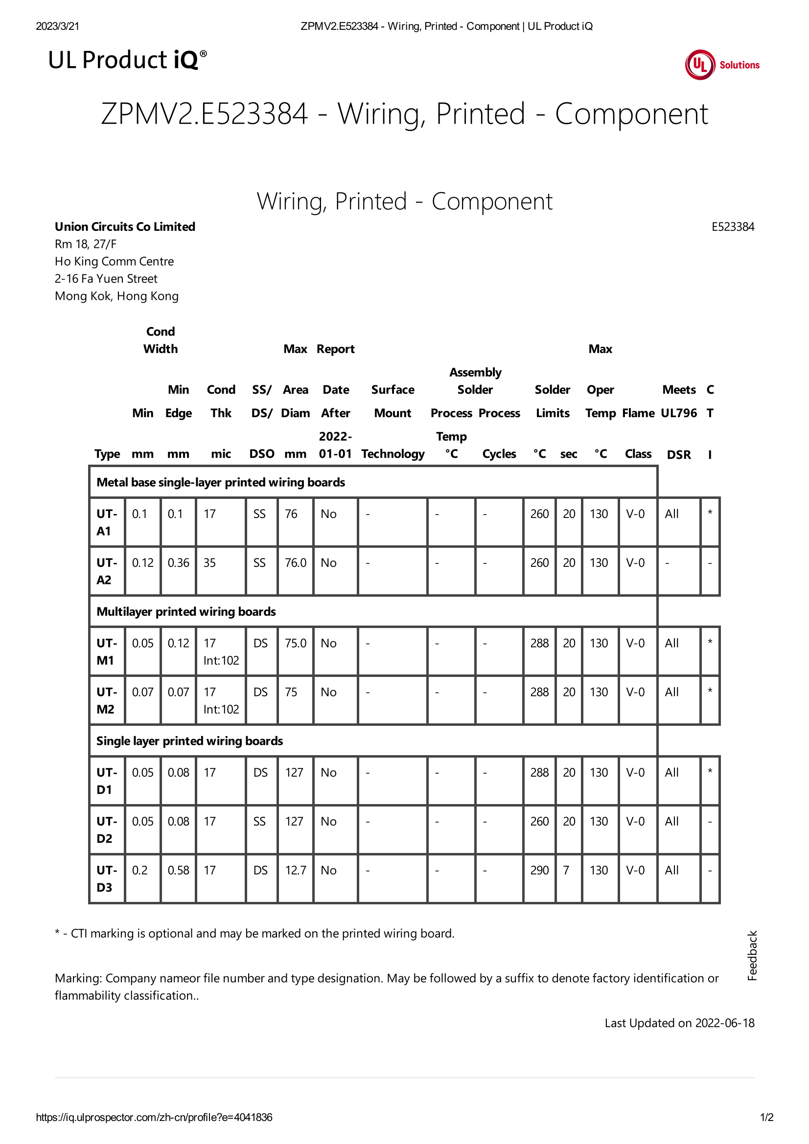
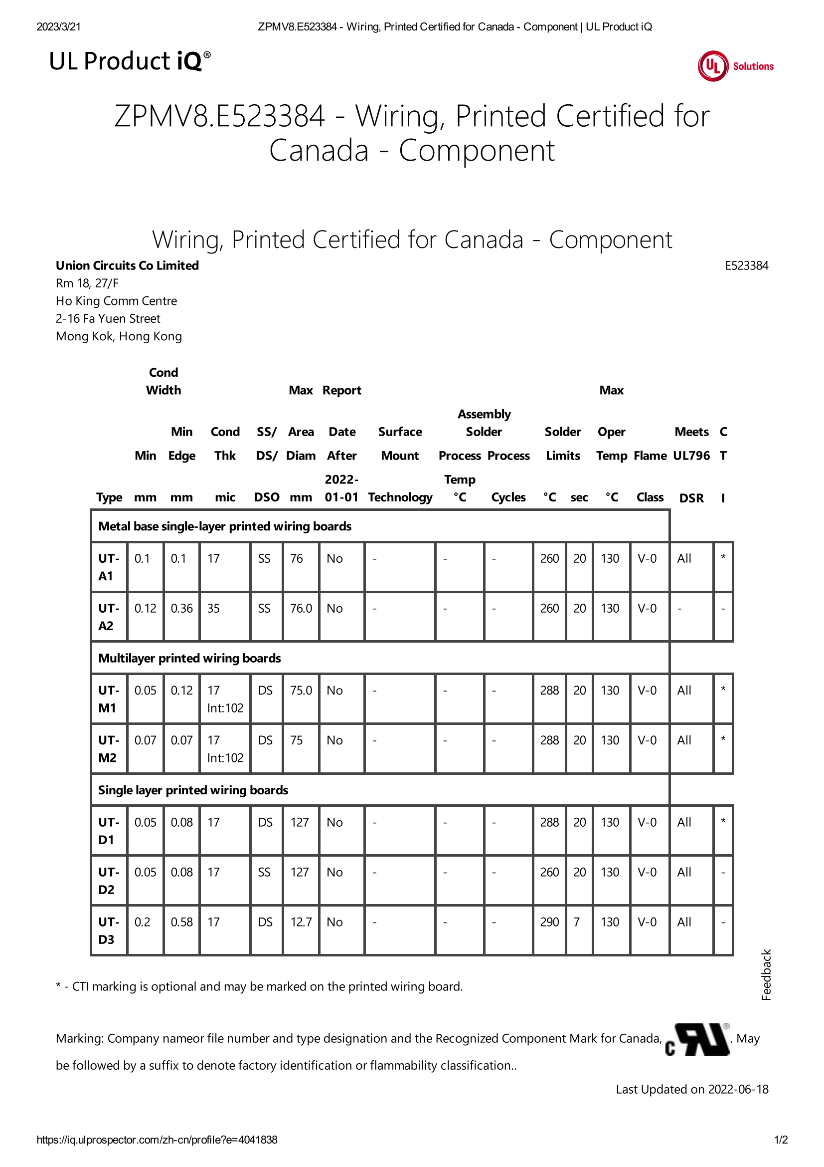
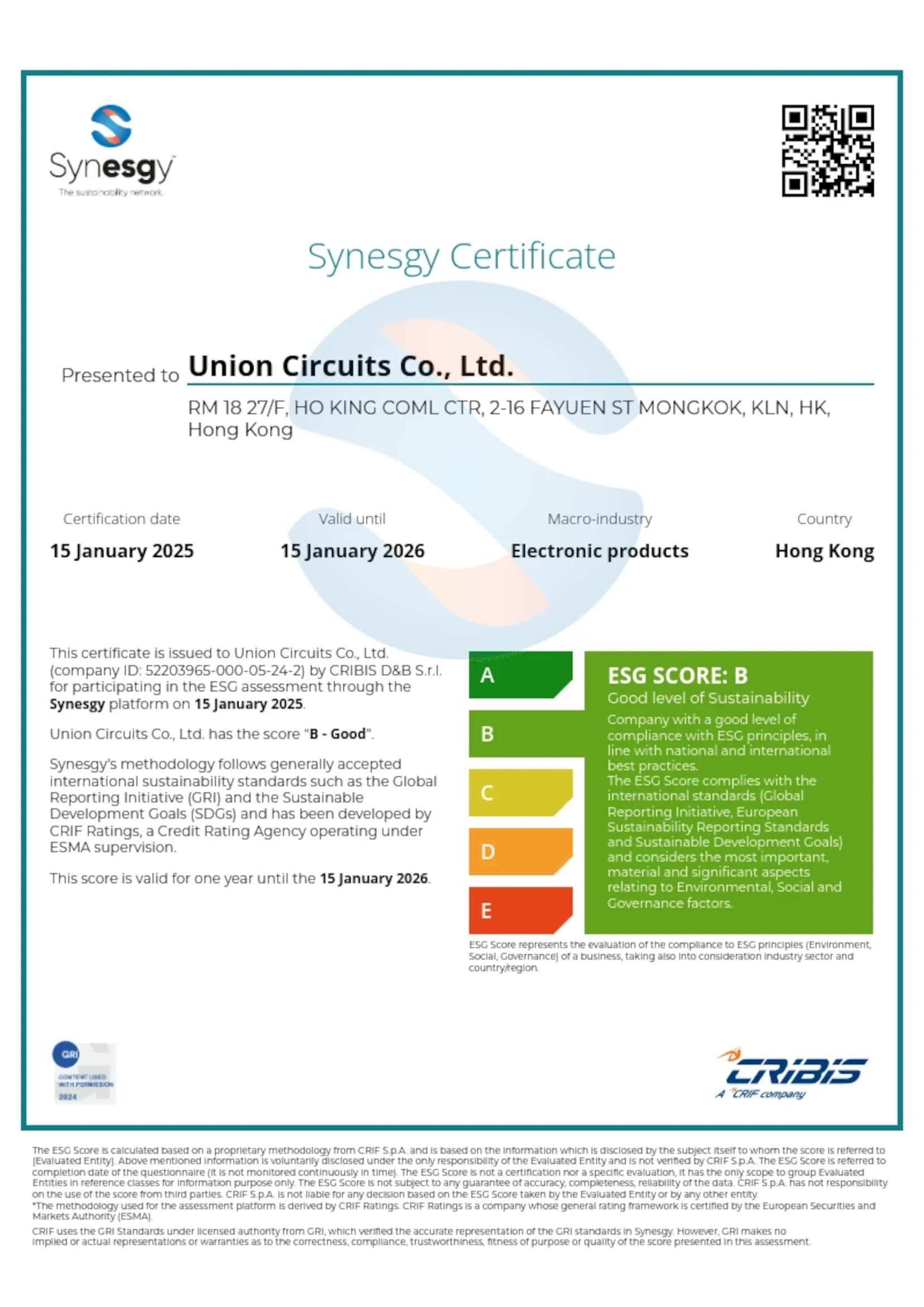
Home > PCB Fabrication
Focus on quick turnaround prototype, small to medium PCB manufacturing since 2010.
Our value-added services are designed to enhance your experience and provide additional benefits beyond our core offerings. From quality guarantees to personalized support, we are committed to going the extra mile to ensure your complete satisfaction.
Ensure the PCB design meets manufacturability criteria to identify potential issues affecting efficiency, quality, and costs.
For prototypes, small batches, and applications where speed is crucial, our quickturn services can significantly reduce your lead time from design to finished product.
High Mix Low Volume PCB production, offering a wide variety of PCBs in small quantities, tailored to meet your specific needs.
Analyzing and recreating the layout and function of a PCB from real PCB sample to understand its design, components, and functionality.
| No. | Item | Feature | Standard | Advanced |
|---|---|---|---|---|
| 1 | Layer Count | Min~Max | 1~16L | 48L(Max.) |
| 2 | Material | Types | FR-4, Aluminum/ Copper-base, Rogers | FR-4(Halogen-free), Arlon |
| 3 | Panel Size | Max | 508 x 610 mm(20”x 24”) | 508 x 1500 mm(20” x 34”) |
| 4 | Finished Thickness | Min~max | 0.2~5.0mm(0.005~0.126”) | 0.2~6.5mm(0.005~0.165”) |
| 5 | Trace Width/ Space | Inner/ Outer layer | 3/3mils(0.075/0.075mm) | 2/2mils(0.05/0.05mm) |
| 6 | Mechanical Drilling | Min | 0.008”(0.20mm) | 0.006”(0.15mm) |
| 7 | Mechanical Drilling | Max | 0.197”(5.0mm) | 0.256”(6.5mm) |
| 8 | Laser Drilling | Min | 0.006”(0.15mm) | 0.004”(0.10mm) |
| 9 | Aspect Ratio | Max | 12:1 | 20:1 |
| 10 | Copper Thickness | Min~max | 0.5~6 OZ | 20 OZ(max) |
| 11 | Solder Mask | Color | Glossy/Matt Green, white, black, red, blue | Yellow, pink, purple |
| 12 | Silkscreen | Color | White, black | / |
| 13 | Surface Finish | Types | HASL, Immersion Gold/ Tin/ Silver, Plating hard Gold, OSP | ENEPIG |
| 14 | Routing | Bit diameter | 0.093”, 0.062”, 0.031” | 0.021” |
| 15 | Profile | Tolerance | ±0.006”(0.15mm) | ±0.004”(0.10mm) |
| 16 | V-scoring | Angle | 30° | 20°/ 45°/ 60° |
| 17 | Plating Hard Gold | Thickness | 0.032”(0.8um) typical | 0.050”(max) |
| 18 | Special Processes | / | Carbon Ink, Peelable Mask, depth controll milling | / |
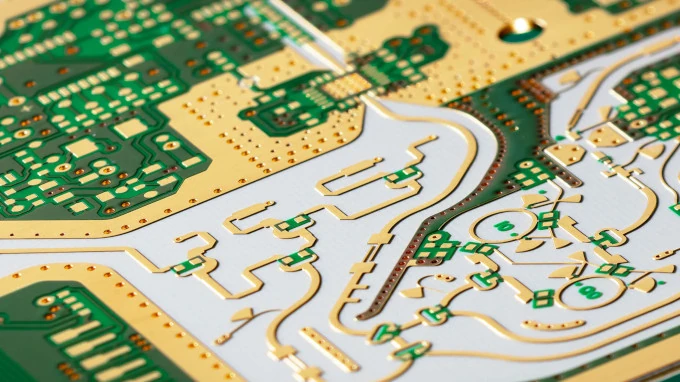
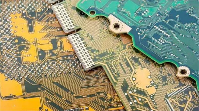
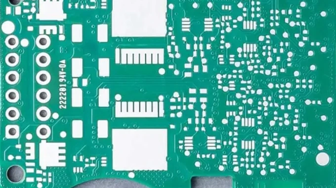
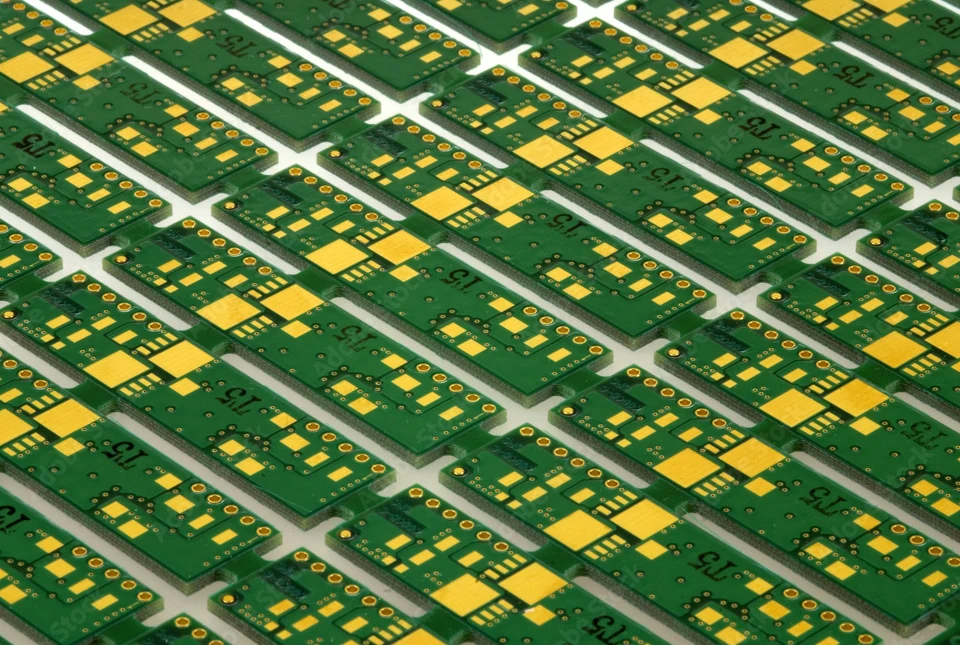
Multilayer PCB manufacturing involves complex processes to create high-density interconnections. Advanced techniques like lamination, etching, and plating are utilized to produce durable, reliable circuit boards that power modern electronics.
Check all the data provided to make sure the designing of the PCB is manufacturable, functional, reliable and cost effective. Raise questions if EQ, then issue MI for production.
Cut the materials into panel according to MI. Including core, Prepreg, copper foils. Tooling holes need to be drilled at this step.
Prepare for the inner layer DFR(Dry Film Resist) lamination. To increase DFR adhesion, etch the surface of copper foils by jet-scrubber, buffbrushing.
Laminate Dry Film on cores. D/F is used as a photosensitive material forphotolithography.
Expose light onto the D/F.LDI (Laser Direct Imaging),which doesn't require mask application,is analternative solution.
Same as the following. Developing the photoresist; Etching away unwanted copper; Stripping the remaining resist to reveal the circuit pattern.
Etch the surface of copper surface to ensure adhesion of coppe and Prepreg.
Laminate Dry Film on cores. D/F is used as a photosensitive material forphotolithography.
Heat the laminated layers under pressure in a vacuum melt Prepreg by heat to multilayer PCB formation. Other processes by the following will be the same as a double-sided PCB.
Drill on board to form through holes.
Remove the smear and resin residues left in the drilled holes, to ensure good electrical connectivity and improve the copper plating quality.
Electroless Copper Plating, a thin layer of copper is deposited on the hole walls through a chemical process, making them conductive.
Electroplating, the thin copper layer is further reinforced with additional copper through electroplating, ensuring robust andreliable electrical connections.
Prepare for the next step, D/F lamination. To increase dry film adhesion, etch the surface of copper foils by jet-scrubber,buff brushing.
Laminate Dry Film on copper foils. D/F is used as a photosensitive material for photolithography.
Apply masks(films) on D/F and expose light onto the surface of copper foils. Currently, we use both ways, D/Fand LDI(Laser Direct Imaging), which doesn't require mask application.
Developing the photoresist; Etching away unwanted copper; Stripping the remaining resist to reveal the circuit pattern.
Use AOI for outer layer inspection, to check for defects such as scratches, misalignments, and incomplete etching, ensuring the final board meets the required specification.
Clean and roughen the copper surface to increase the adhesion between the copper surface and solder resist.
Apply photosolder resist on one side then pre-baking, then printing solder resist on the other side, pre-baking, then exposure-develop-curing.
Screen printing or injet printer printing the legend.
Apply surface treatment according to the specification, like Lead-free HASL, OSP, Immersion Gold/Tin/Ag etc.
CNC routing, V-scoring, or punching, to de-panel the board from working panel.
Use Probe flying testing for prototype and small series, and E-test fixture for production orders.
Final Quality Control and Final Quality Assurance for the finished PCB.
Packing according to the specification and ship to worldwide customers.
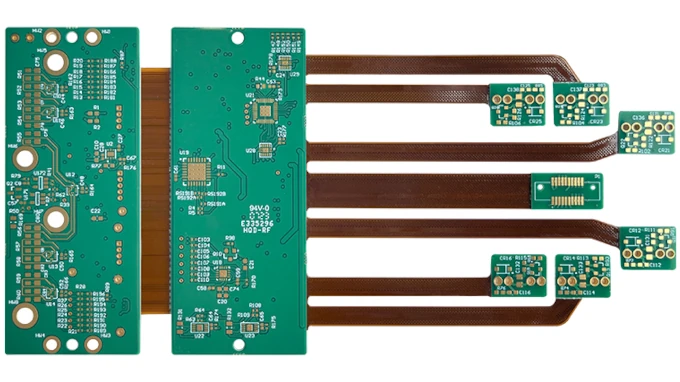
Multi-layer PCB leads in both market share and revenue, reflecting industry trends toward more complex, high-performance electronics. The increasing demand for consumer electronics, IoT devices, and automotive applications continues to boost the multi-layer PCB market significantly.
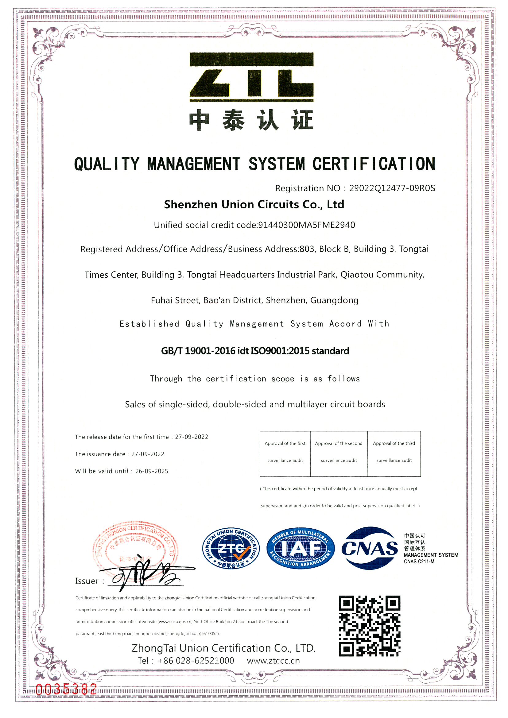
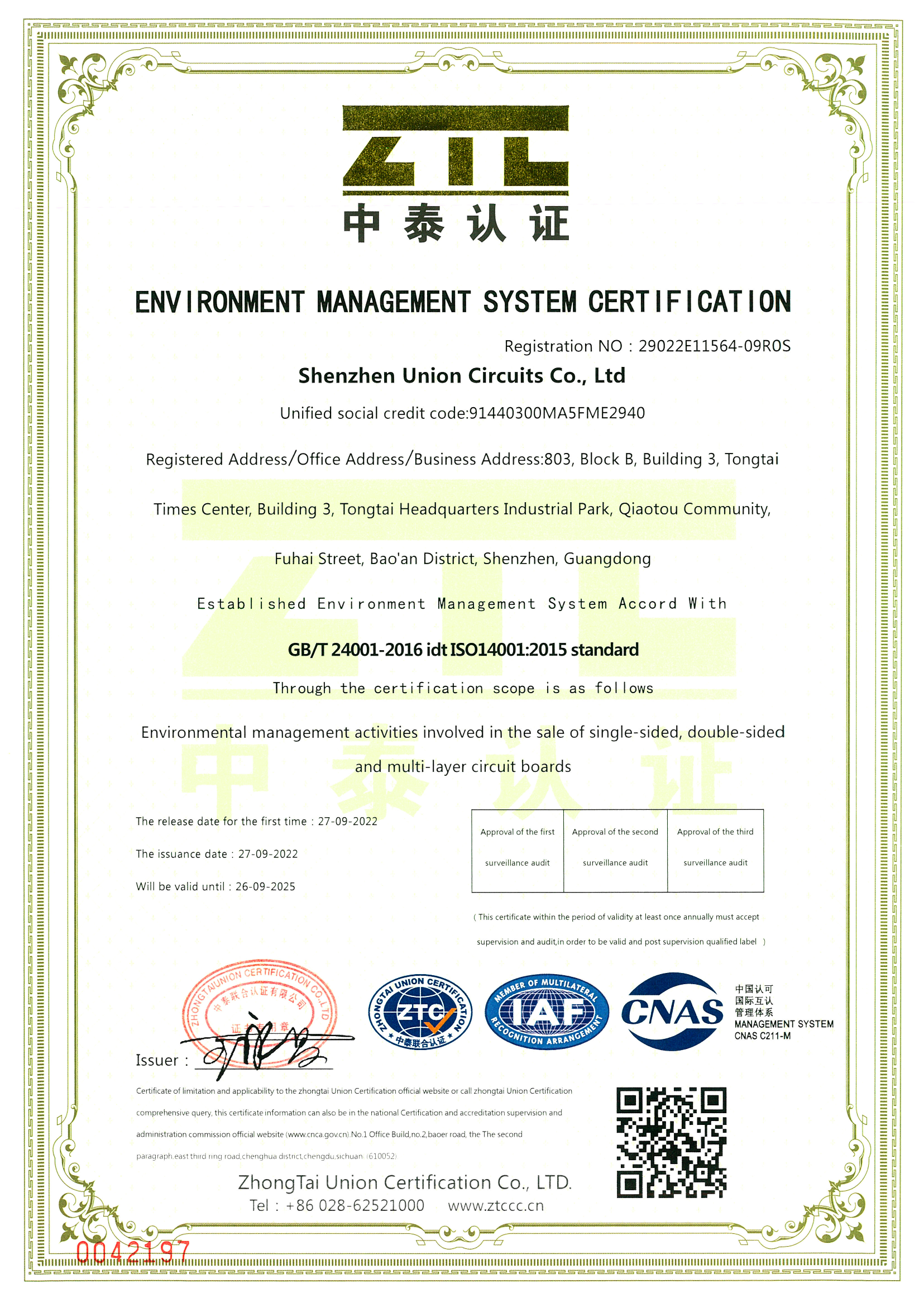
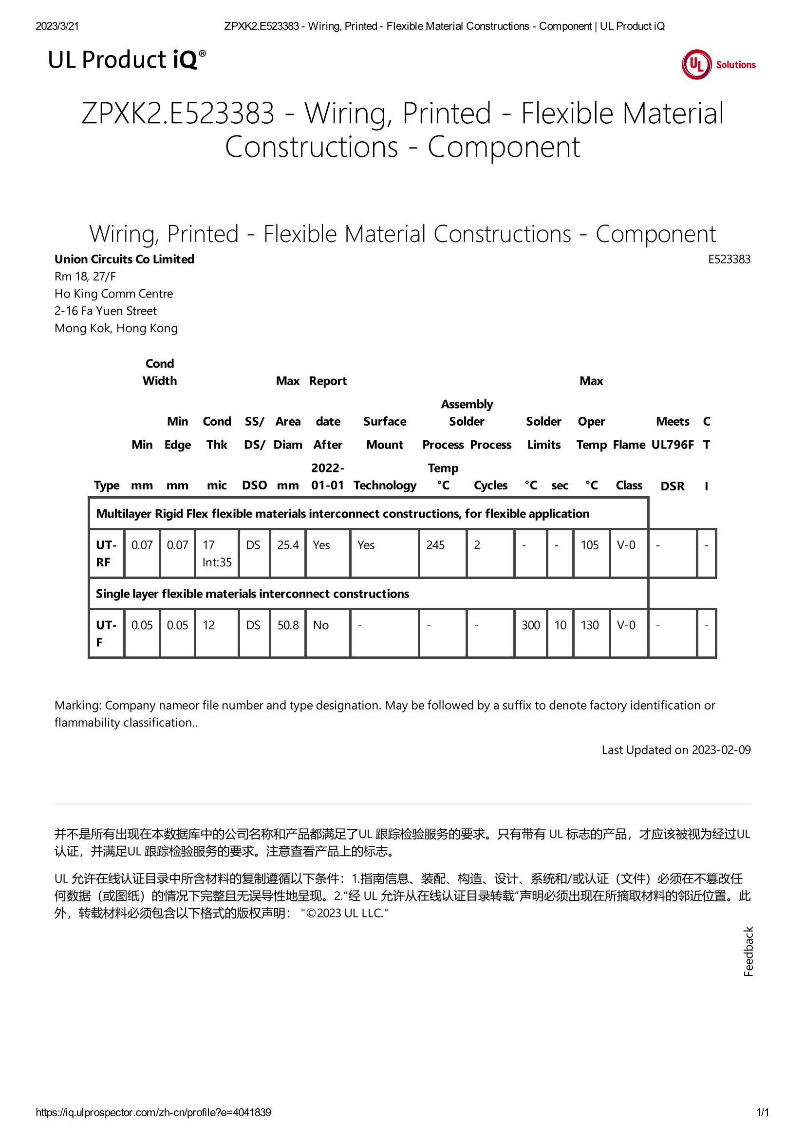
In-depth and comprehensive overview of PCB industry standards and best practices required for ensuring quality assurance and consistency across all production processes.