Home > PCB Fabrication > Multilayer PCB
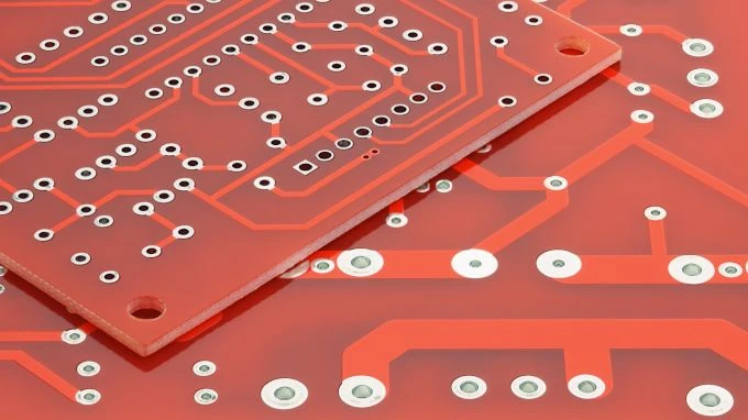
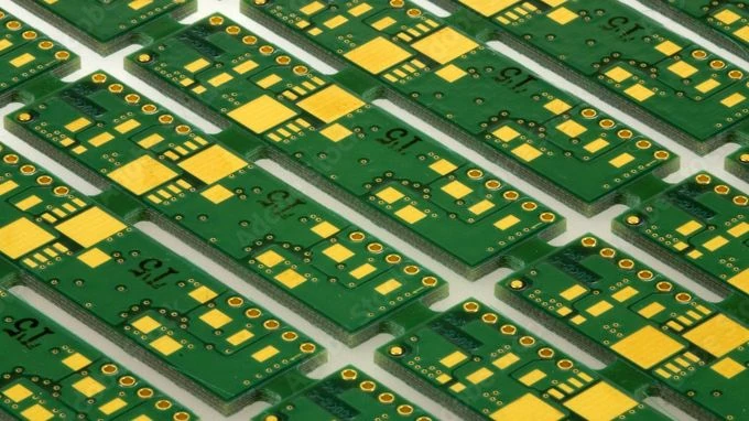
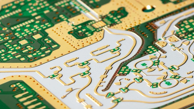
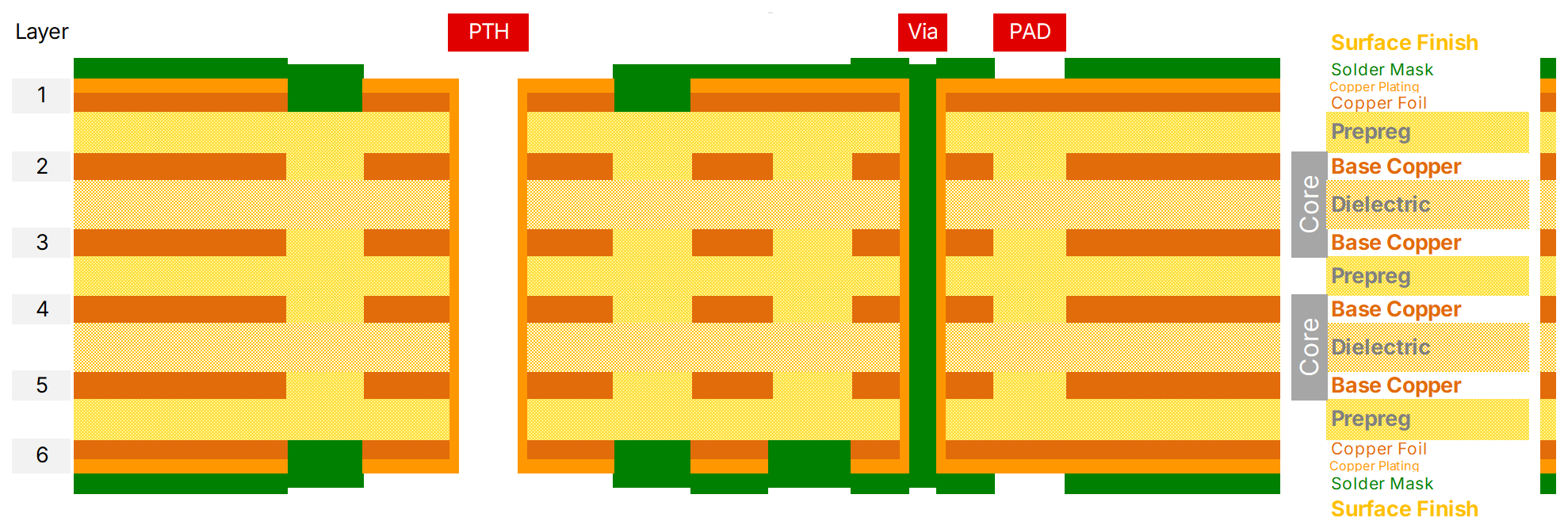
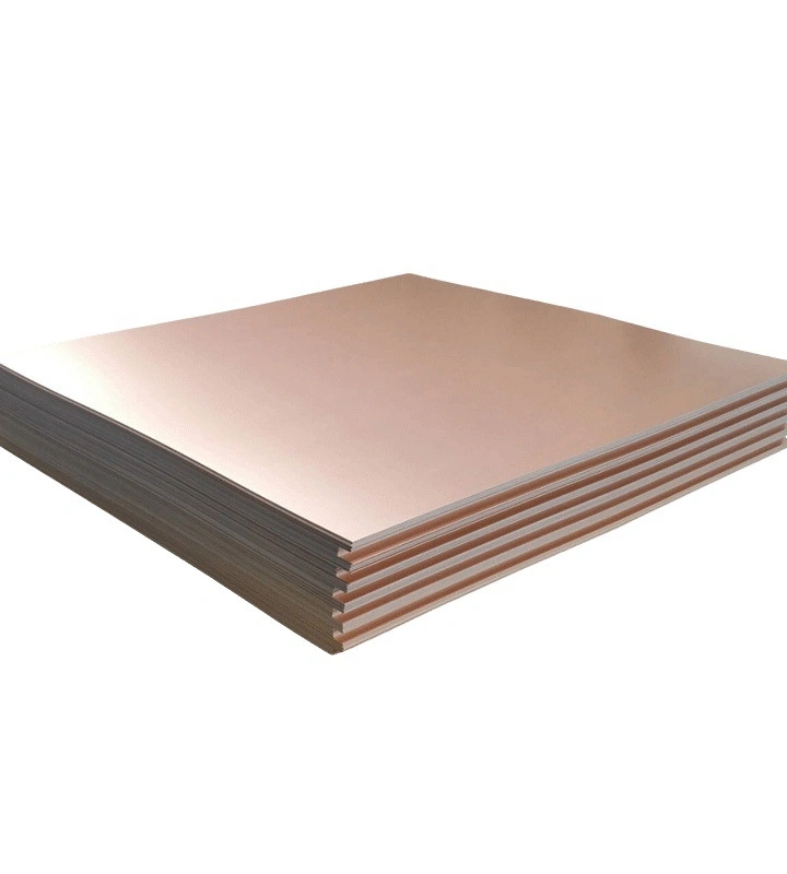
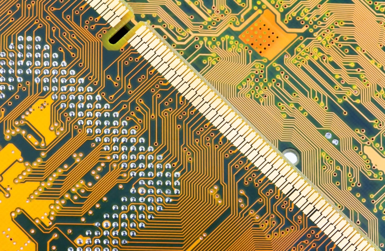
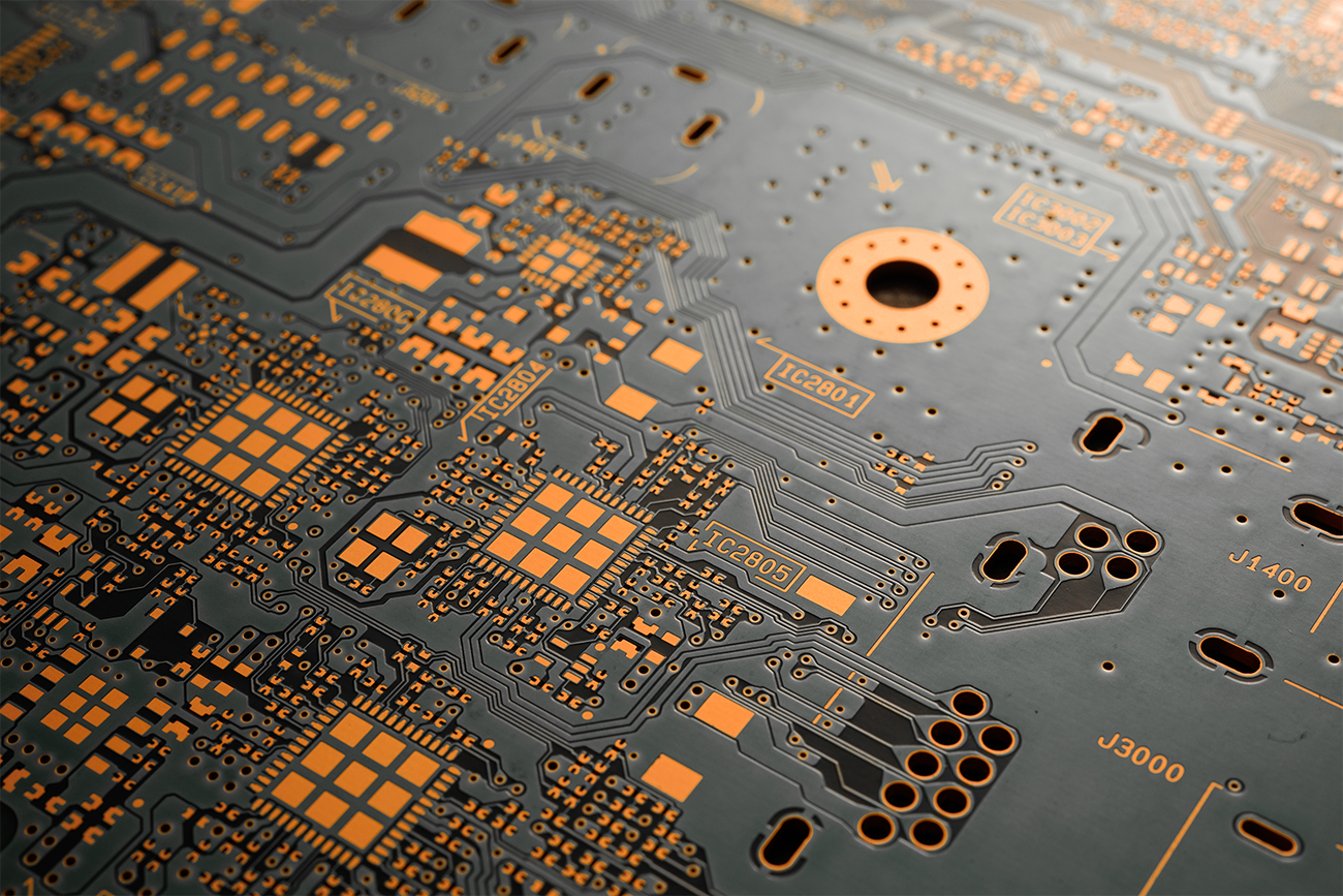
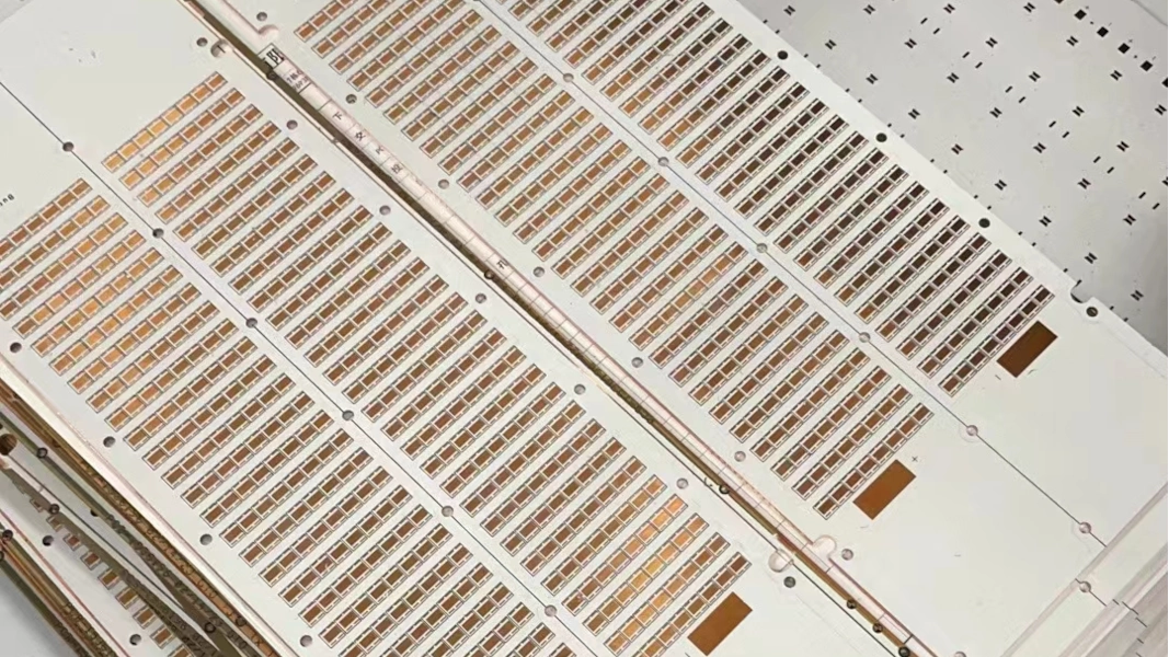
Multilayer PCB consists of multiple conductive copper layers separated by insulating layers, commonly configured with 4, 6, 8 layers and so on. These layers are bonded together using heat and adhesive to form a single, integrated board. The inner layers are made of a substrate material known as the core, and the insulating layers are often referred to as prepreg. Prepreg is a glass-reinforced epoxy material impregnated with resin, and it facilitates the bonding of copper layers. Connections between outer and inner layers are established via plated through holes (PTH) and vias. Multilayer PCB introduces the lamination process, which is where we actually creates the composite PCB from layers of circuitry in a lamination press under high pressure and heat. After pressing, multilayer PCB production is treated almost the same as a traditional double-sided PCB.
The effectiveness and reliability of multilayer PCBs depend on the careful selection and processing of core materials, copper foils, and prepreg. Each component must be optimized to work together, ensuring structural integrity, electrical performance, and manufacturability throughout the production cycle.
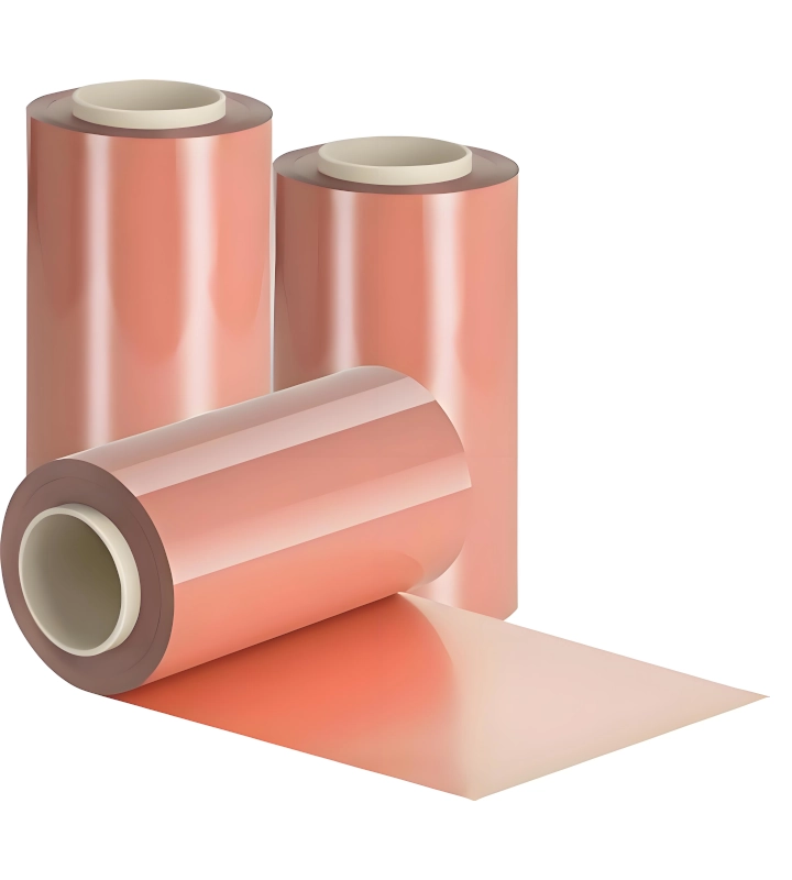
Role: Copper foil provides the conductive pathways in the PCB, and its quality directly affects circuit integrity, plating, and lamination.
Types & Sheets: Rolled-annealed or electrolytic copper foils are used, with specifications focusing on thickness, surface finish, and cleanliness.
Processing: Copper foil is laminated onto prepreg or core by stacking and pressing under heat and pressure. The foil’s surface finish and adhesion properties influence reliability, especially during plating and etching.
Critical Aspects: Uniform thickness, smooth surface, and good adhesion to the dielectric layer are critical for high-density circuitry and precise impedance control.
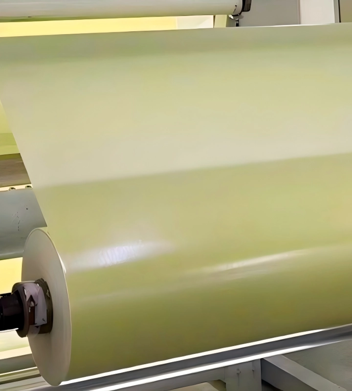
Purpose: Prepreg acts as an adhesive layer, bonding cores and copper foils together in multilayer stackup.
Material Composition: Partially cured resin system (usually epoxy), reinforced with glass fibers, designed to flow and cure during lamination.
Processing: Prepreg is laid up between cores and copper foils, then pressed under controlled heat and pressure, allowing resin flow and bonding. Proper curing ensures mechanical strength and electrical insulation.
Key Features: Its resin content, glass content, and Tg influence the uniformity of bonding, dimensional stability, and thermal performance during manufacturing and operation.
Function: The core provides the foundational dielectric layer in multilayer PCBs, typically consisting of a laminate with dielectric materials bonded to copper foil on both sides.
Material Composition: Usually made from glass-reinforced epoxy resin (like FR-4) cured and stabilized to ensure dimensional stability.
Processing: Cores are manufactured through lamination processes involving controlled temperature, pressure, and resin cure cycles to achieve uniform thickness and stability, critical for maintaining layer alignment and impedance control.
Key Considerations: The core’s physical and electrical consistency influences the overall performance, and its behavior during lamination impacts subsequent layer bonding and the laminate’s dimensional stability.
PTH(Plated-through-hole) technology is used in printed wiring boards (PWBs) to create electrical connections between different layers by metallizing the holes drilled through the boards. This method has been in practice since the mid-1950s and has undergone significant advancements over the decades.
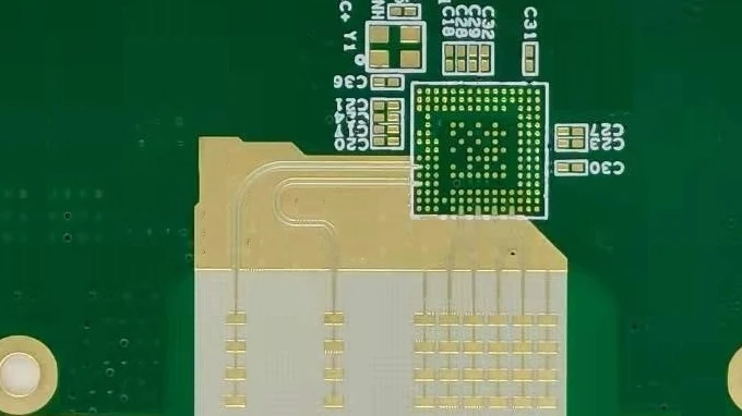
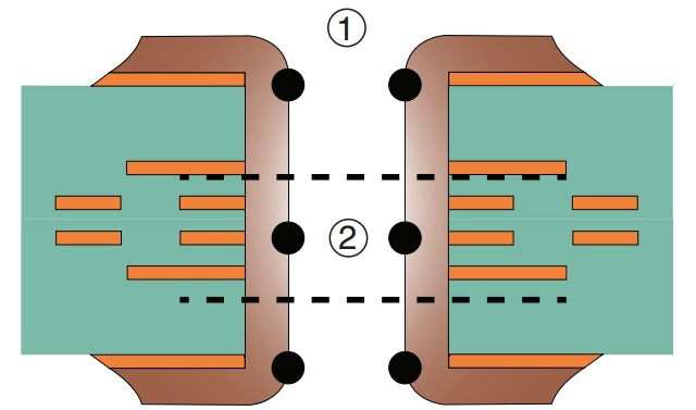
Via is a plated-through hole that connects different layers of a multilayer board, enabling electrical signals to pass between layers. Types include through-hole, blind, and buried vias. They can also be filled or capped for added reliability. The quality and reliability of vias are critical, as defects can cause board failures, especially in high-density or mission-critical applications. Standards like IPC-4761 provide guidelines for via design and protection.
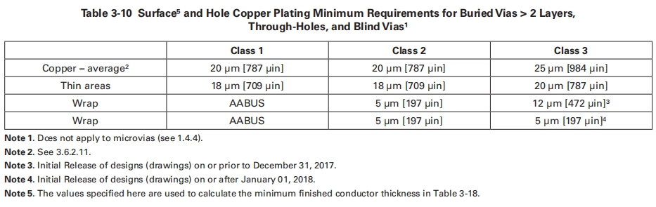
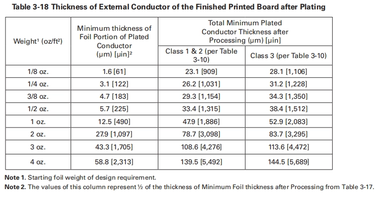
Hole copper plating thicknesses shall meet the requirements of Table 3-10 through Table 3-12, shall be continuous and shall extend or wrap from hole walls onto outer surfaces (Refer to IPC-A-600 for discussion on copper plating thickness for hol walls). Deviations to these requirements shall be AABUS. Each side of the plated hole wall shall be evaluated independently. Measurements of the plating thickness shall be reported as an average thickness of 3 measurements per side of the hole. At least one measurement shall be taken within 40 – 60% of the hole height. Isolated thick or thin sections shall not be used for averaging. Isolated areas of reduced copper thickness due to glass fiber protrusions shall meet the minimum thickness requirements of Table 3-10 through Table 3-12 as measured from the end of the protrusion to the hole wall.
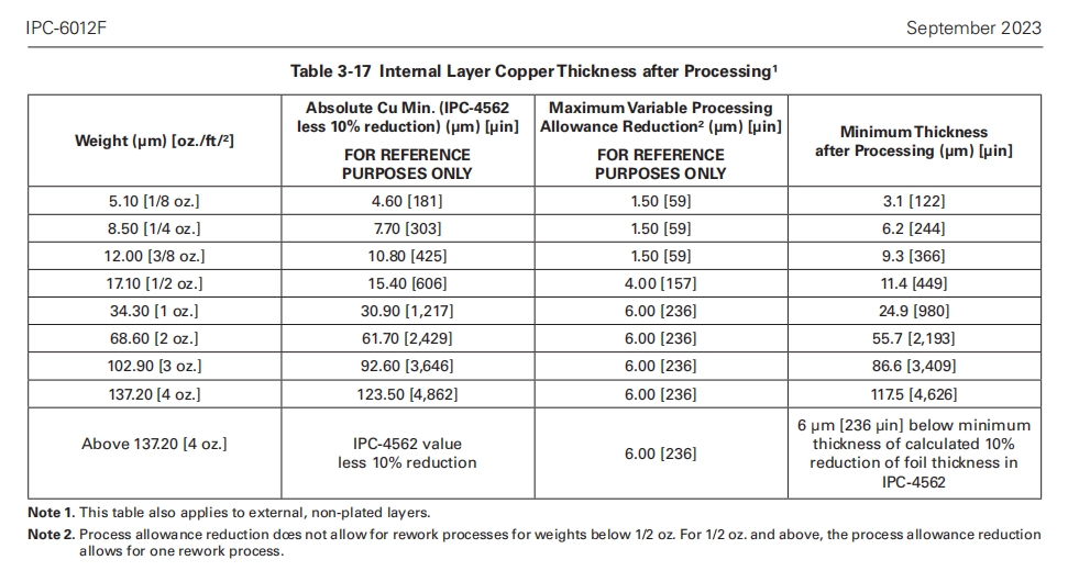
If the internal conductor thickness of the finished printed board is specified by a foil weight, the minimum internal copper foil thickness after processing shall be measured in accordance with Table 3-17 for all classes. When the procurement documentation specifies a minimum copper thickness, the conductor shall meet or exceed that minimum thickness.
The requirements in Table 3-17 are based on minimum copper foil thickness allowances per IPC-4562 followed by two successive scrubbings. Each scrub is expected to remove a specific amount of copper and is represented by a variable processing allowance reduction.
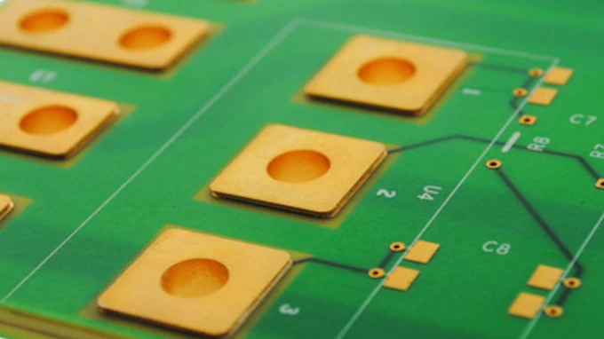
Soldermask is a thin protective coating applied to the surface of a PCB to insulate copper traces from environmental factors and prevent accidental solder bridges during component soldering. It is usually green but can come in other colors and plays a crucial role in enhancing PCB durability, reliability, and manufacturability by preventing short circuits and corrosion. Soldermask key functions:
Soldermask masks off and insulates the non-pad copper areas, preventing accidental solder bridges between adjacent pads or traces during soldering.
It shields the copper from oxidation, dust, moisture, and contaminants, enhancing the PCB’s durability and reliability over time.
Provides electrical insulation between conductors and protects the surface from physical damage and environmental stress.
Improves solder wetting and solder joint quality by clearly defining where solder should be deposited.

Most PCBs use copper as their primary conductor. If the copper is left unprotected after finishing, it can oxidize, making soldering difficult. An ideal surface finish would possess good solderability, a flat coplanar surface, cost-effectiveness, the ability to withstand unlimited heat cycles, and minimal health and safety concerns. There are various final finishes available, each with its own advantages and disadvantages. Different finishes are more suitable for specific applications.
OSP is exceptionally thin organic coatings specifically formulated to preserve the solderability of copper surfaces on PCB. This coating works by forming a complex organo-metallic bond with the copper, which is critical for ensuring a reliable solderable finish. OSP is particularly suitable for a range of applications, including both surface mount and through-hole assembly processes. Additionally, they offer a shelf life that supports effective long-term storage without compromising solderability, making them a practical choice for manufacturers and engineers alike.
Hot Air Solder Level (HASL or HAL) is the process of immersing a circuit board into molten solder, immediately followed by blowing the excess molten solder out of the holes using hot air under high pressure. For the vast majority of HASL applications, the solder alloy is tin-lead. For Pb-free applications, the main alloys include tin-copper, tin-silver-copper, tin-copper-nickel, and tin-copper-nickel-germanium alloys.
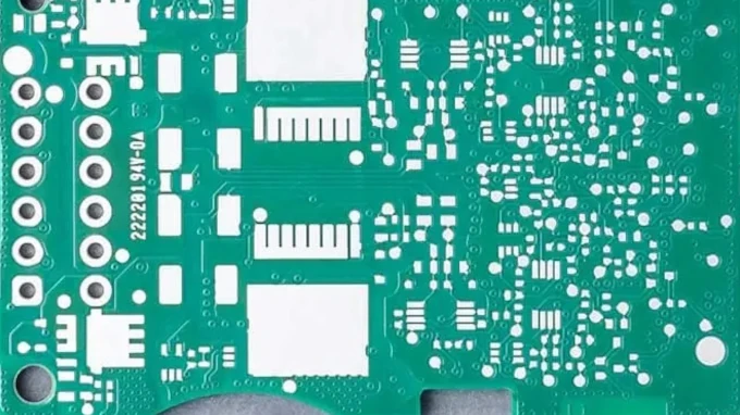
Discover the versatility of Multilayer PCBs, designed for high-performance applications. Explore various configurations to meet the demands of modern electronics, ensuring reliability and efficiency for diverse industries.
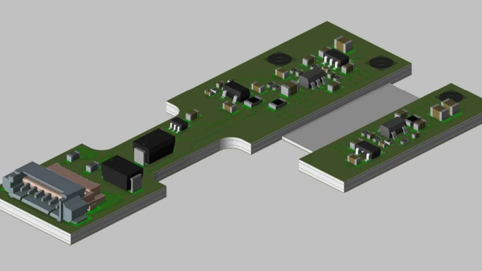
Unlock your potential with the unique strength and flexibility of multilayer aluminum-based PCBs! Our innovative and carefully designed solutions will enhance your projects, offering excellent thermal management and improving performance in various electronic applications. Stay on the cutting edge of technology and discover the impressive advancements of our multilayer PCB solutions, built to meet the changing demands of today’s tech world. Learn how these advanced PCBs can elevate your projects and make your electronic devices more efficient and reliable. Let’s embark on this exciting journey to success together!
Embrace the limitless potential of advanced multilayer copper-based PCBs, which are designed to meet the demanding needs of modern electronic applications. Our pioneering technology not only inspires unmatched performance but also guarantees exceptional reliability for all of your visionary electronic designs. By choosing our cutting-edge multilayer PCB solutions, you can truly transform your projects and bring your ideas to life. Experience the freedom to innovate and let your ideas soar to new heights with our industry-leading technology, crafted to support the complexities of your most ambitious projects. Whether you’re developing consumer electronics, industrial systems, or groundbreaking technological solutions, our multilayer PCBs are the ultimate foundation for success.
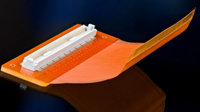
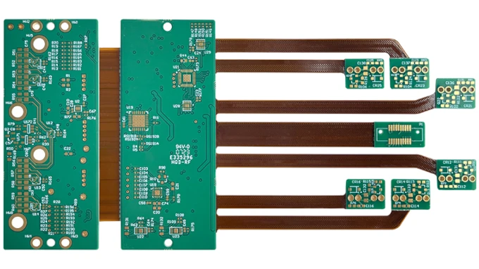
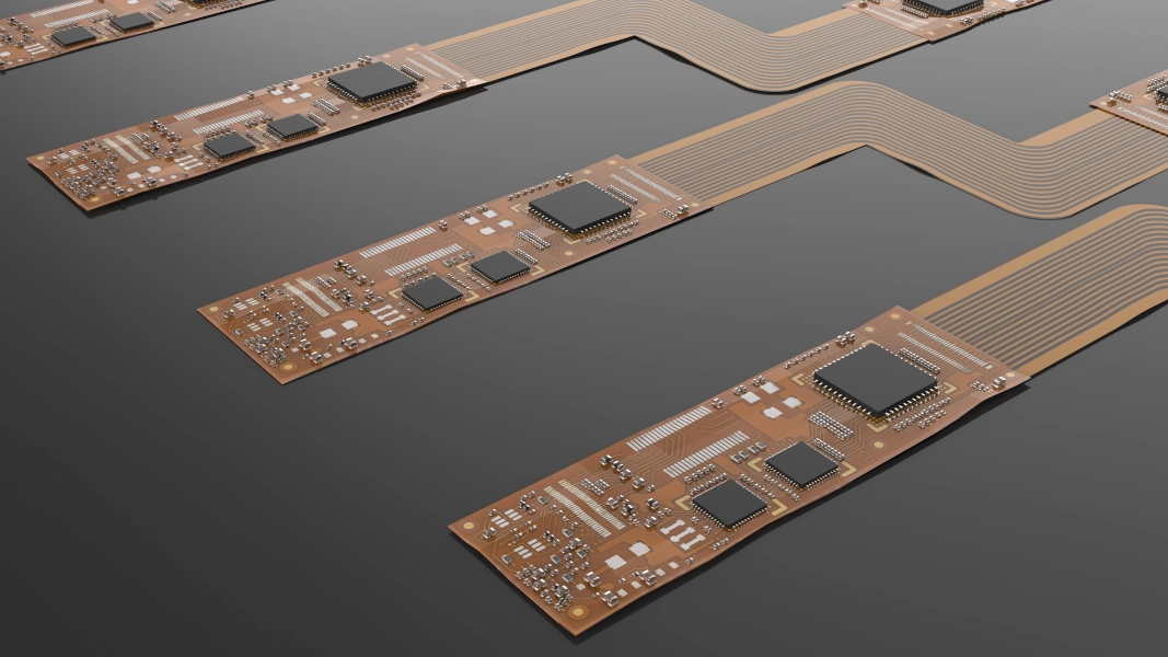
Unleash your potential with the groundbreaking capabilities of multilayer flexible printed circuits (FPC), empowered by our innovative technology. Venture into the extraordinary design features and cutting-edge manufacturing processes that enable the effortless integration of multilayer printed circuit boards (PCBs). Our visionary approach guarantees exceptional performance and unwavering reliability, making it the ultimate choice for your varied electronic aspirations and intricate projects. Embrace the future of circuit technology and witness how our pioneering solutions can elevate your product’s efficiency and functionality to unprecedented levels.
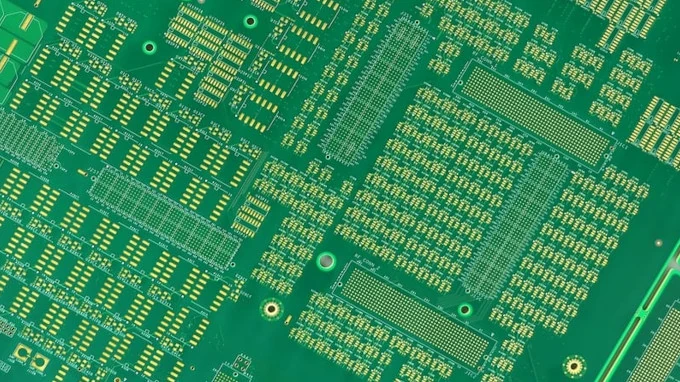
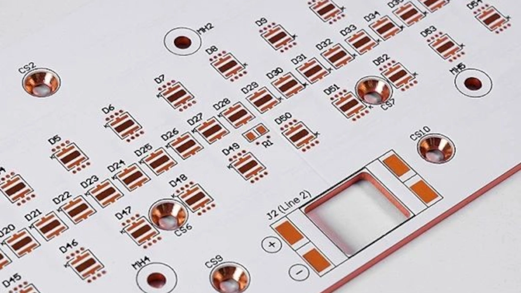
Essential information includes part numbers, fabrication and drill drawings, manufacturing notes, board details, material specifications, conductor patterns, artwork data for both sides, aperture lists, drill data, netlist data, and any special requirements.
Designers focus on layer count optimization, power/ground plane placement, controlled impedance routing, signal isolation, thermal dissipation, and via structures (blind, buried, or through-hole) for reliable connectivity.
Typical layer counts are 4 to 8 layers, common for consumer electronics and networking and telecom devices.
Typical materials include prepreg (pre-impregnated dielectric sheets), core substrates made from fiberglass-reinforced laminates like FR-4 or specialized materials for high-speed/high-frequency applications, and copper foils. Advanced multilayer PCBs may also use high-speed dielectric substrates like Rogers or PTFE-based materials for specific electrical properties.
Proper layer stacking, controlled impedance routing, and short signal path design help minimize signal reflections, crosstalk, and electromagnetic interference. Careful via placement and ground plane design are critical for maintaining high-speed signal quality and reducing noise.
Higher component density (saves space), improved signal integrity (reduced EMI and crosstalk), better power distribution (dedicated power and ground planes), enhanced durability (rigid structure).
Number of layers (more layers = higher cost), material selection (high-frequency or exotic materials cost more), Via types (blind/buried vias increase cost), tolerances & testing (tight specs require more QA).
Consumer electronics, telecom equipment, aerospace avionics, medical imaging devices, automotive radar systems, and industrial automation heavily rely on multilayer PCB technology.
Electrical testing detects opens/shorts, AOI checks for surface defects, microsection analysis verifies inner-layer integrity, and X-ray inspection ensures proper via filling and solder joint quality.
High layer counts increase board thickness and thermal mass, making reflow soldering more complex. Warpage, fine-pitch BGA soldering, and mixed SMT/through-hole components also require precise assembly techniques.
Common FAQ topics. If you have specific questions in mind, feel free to ask!