Home > HDI PCB
High Density Interconnect (HDI) PCBs are advanced circuit boards characterized by a higher line density than traditional PCBs. They employ micro blind and buried via technologies, essential for meeting the electrical demands of high-speed signals. The development of these boards is driven by the need for impedance control with alternating current characteristics, high-frequency transmission, and minimizing electromagnetic interference (EMI). Utilizing Stripline and Microstrip structures, HDI PCBs often feature multi-layer designs. These boards use insulating materials with low dielectric constants and attenuation rates to enhance signal transmission quality.
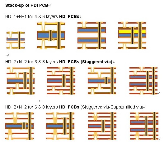
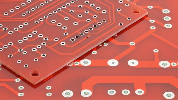
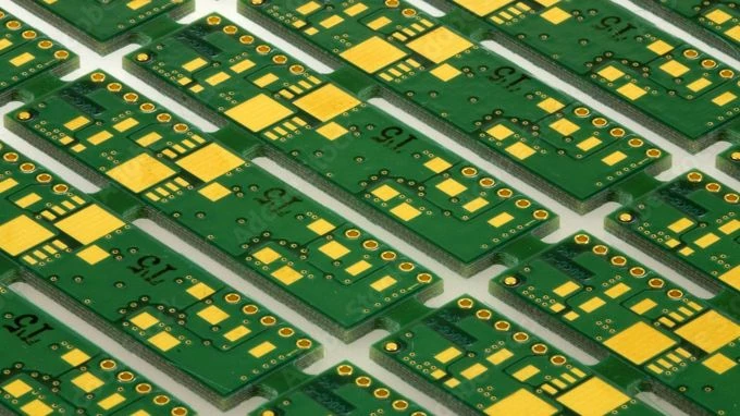
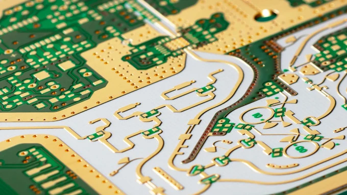
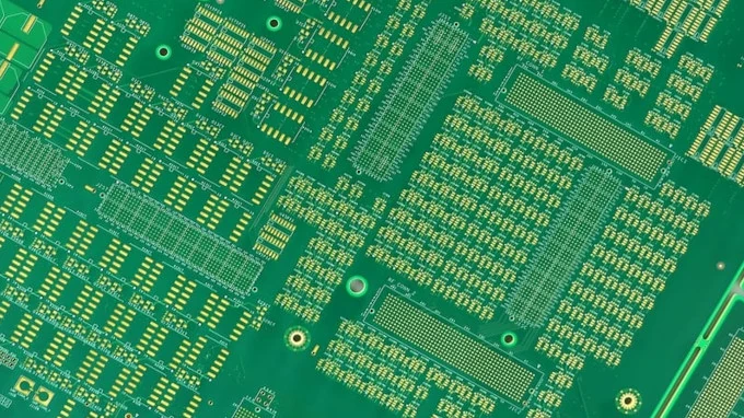
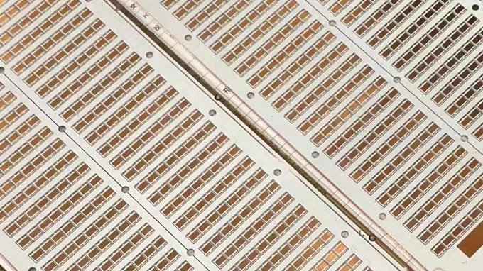
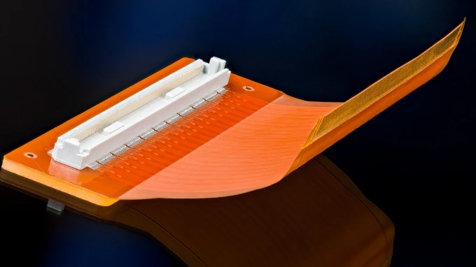
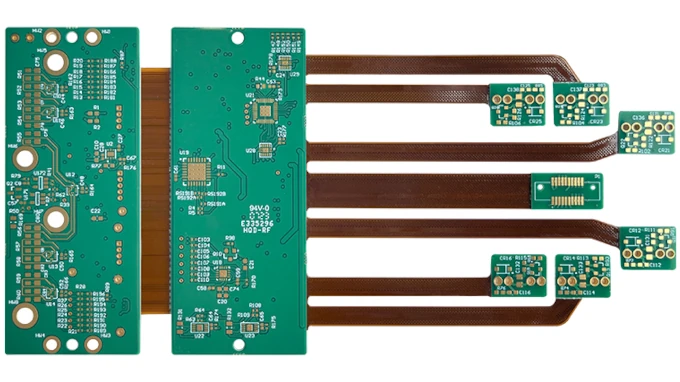
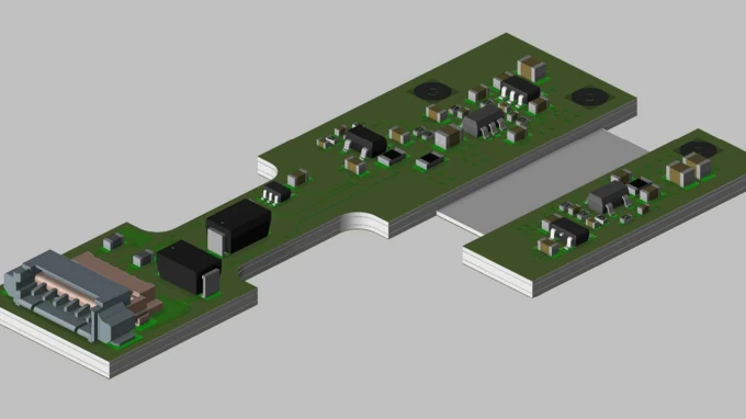
HDI PCB laminates are specialized materials designed to support high-density interconnect (HDI) and microvia technologies. These laminates must possess exceptional dimensional stability, thermal stability, and compatible dielectric properties to ensure reliable manufacturing and high-performance electrical characteristics. Below are the key Characteristics of HDI Laminates:
HDI laminates typically utilize advanced resin systems, such as epoxy-based or polyimide resins, combined with reinforcements like glass fabrics. They often incorporate special reinforcements, including very thin or low-loss glass cloths (e.g., 1037, 1027, 1017), to achieve the necessary thinness and electrical performance.
The rheology (flow behavior) of the resin is vital for achieving proper lamination and via filling. Parameters such as resin melting and curing points, viscosity profiles, and resin flow characteristics are critical for process optimization.
Microvia laminates often have resin systems tailored for laser ablation and plasma etching processes used to form microvias. They may incorporate resin-coated copper foils with B-stage (partially cured) or C-stage (fully cured) resins to facilitate via formation and filling.
HDI applications demand excellent dimensional stability to maintain layer registration, especially as the number of layers increases and via sizes decrease. Materials are engineered to minimize warping or shrinkage during processing and thermal cycling.
High decomposition temperature, thermal stability, and mechanical robustness are essential to withstand multiple reflow cycles, especially under lead-free and RoHS-compliant processes that involve higher temperatures.
HDI laminates conform to standards such as IPC-4104 and IPC/JPCA-4104, which specify classification, conformance, and quality assurance for materials intended for high-density interconnect applications.
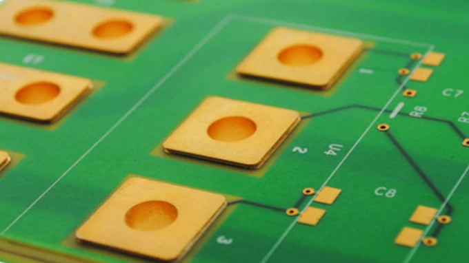
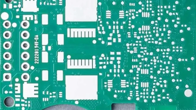
HDI PCB laminates are advanced, low-loss, and dimensionally stable materials that support microvias and fine features. Their selection depends on process compatibility, electrical performance, and reliability considerations, aligning with industry standards for high-density, high-reliability applications like mobile devices, smartphones, and high-speed electronics.
Hole copper plating thicknesses shall meet the requirements of Table 3-10 through Table 3-12, shall be continuous and shall extend or wrap from hole walls onto outer surfaces (Refer to IPC-A-600 for discussion on copper plating thickness for hol walls). Deviations to these requirements shall be AABUS. Each side of the plated hole wall shall be evaluated independently. Measurements of the plating thickness shall be reported as an average thickness of 3 measurements per side of the hole. At least one measurement shall be taken within 40 – 60% of the hole height. Isolated thick or thin sections shall not be used for averaging. Isolated areas of reduced copper thickness due to glass fiber protrusions shall meet the minimum thickness requirements of Table 3-10 through Table 3-12 as measured from the end of the protrusion to the hole wall.
Aspect ratio (hole diameter to board thickness ratio), most suppliers specify an aspect ratio requirement ranging from 0.6:1 to 1:1, with the most common being 0.8:1. For example, a dielectric thickness of 80 µm with a laser drill diameter of 0.1 mm represents an aspect ratio of 0.8:1.
HDI constructions are classified based on the number of lamination and laser drilling steps required:
Any layer HDI PCBs, sometimes referred to as ELIC (Every Layer Interconnect) PCBs, are a type of PCB where every layer can connect to any other layer.
An HDI PCB (High-Density Interconnect) is a printed circuit board with finer trace widths, smaller vias, and higher wiring density than conventional PCBs. It uses microvias, sequential lamination, and laser drilling to achieve compact designs with improved electrical performance.
HDI PCBs offer miniaturization, reduced signal loss, higher routing density, and better performance in high-frequency applications. They also allow designers to use fewer layers while maintaining advanced functionality.
Designers must plan for smaller vias, controlled impedance, fine-line routing, and optimized layer stack-ups. They also need to manage thermal and electrical performance while adhering to DFM guidelines to maintain yield.
HDI boards use sequential lamination, laser drilling for microvias, copper filling for stacked vias, and advanced imaging techniques like LDI to define fine features with high accuracy.
HDI laminates have thinner layers, lower resin content, and specialized resin systems to support fine features, better dimensional stability, and enhanced electrical performance compared to standard FR-4.
Yes. Additional lamination cycles, advanced drilling equipment, fine-line imaging, and yield challenges increase cost. However, the miniaturization and performance benefits often justify the price for high-end electronics.
Challenges include managing resin flow during lamination, ensuring microvia reliability, maintaining dimensional stability, and preventing defects like delamination or conductive anodic filament (CAF) growth.
HDI PCBs are widely used in smartphones, tablets, medical implants, aerospace, automotive radar systems, industrial controls, and high-speed communication devices like 5G equipment.
IPC-2226 (HDI design standards), IPC-6012 (qualification specifications), and IPC-6018 (high-frequency performance) provide guidelines for HDI PCB reliability, manufacturability, and performance verification.
Fine-pitch BGAs, tiny components, and ultra-thin boards demand precise placement, controlled solder paste application, and carefully managed reflow profiles to prevent solder bridging or warpage.
Common FAQ topics. If you have specific questions in mind, feel free to ask!