HDI2
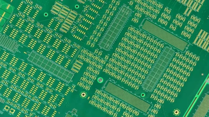
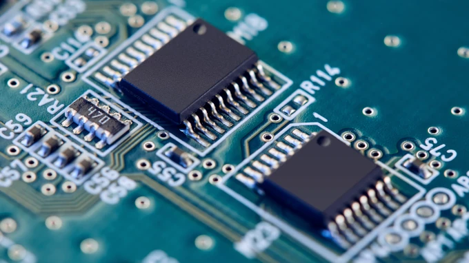
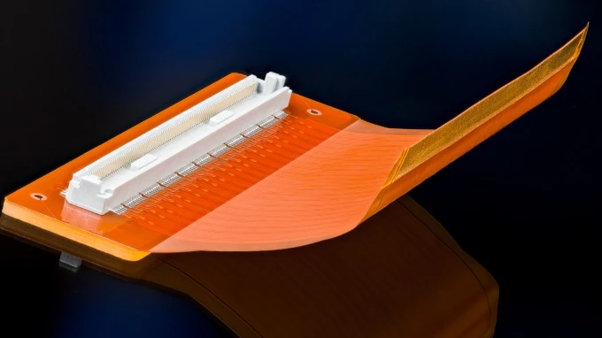
HDI PCB Key Features High-Density Interconnect (HDI) PCBs are advanced circuit boards designed for complex, high-density electronic assemblies. The key features of HDI PCBs include: 1. Microvias and Laser Drilling HDI PCBs utilize microvias—small-diameter vias typically drilled with laser technology—to create interlayer connections. These microvias are often only a few mils in diameter and allow for high interconnection density while preserving space for routing. 2. Blind and Buried Vias HDI technology incorporates blind vias (connecting outer layers to internal layers without passing through the entire PCB) and buried vias (restricted to internal layers), which enable more routing channels and reduce via count