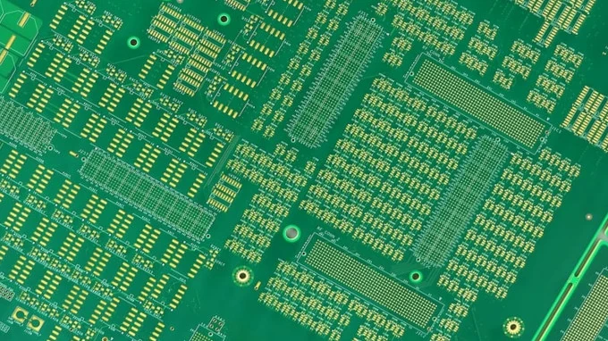
HDI PCB Key Features High-Density Interconnect (HDI) PCBs are advanced circuit boards designed for complex, high-density electronic assemblies. The key

HDI PCB Key Features High-Density Interconnect (HDI) PCBs are advanced circuit boards designed for complex, high-density electronic assemblies. The key
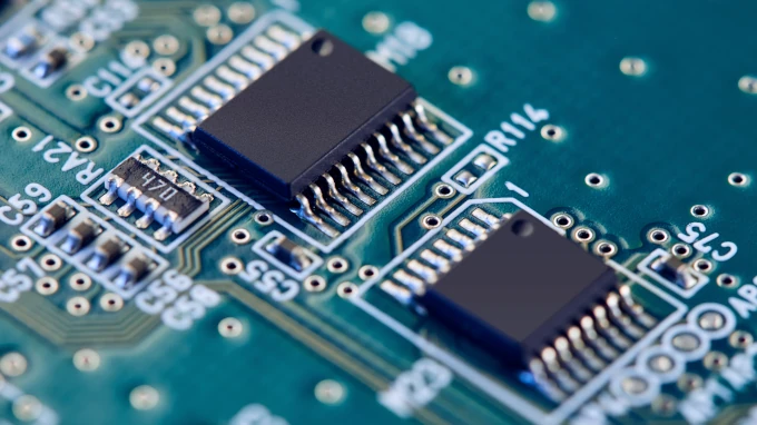
Lead-free HASL (Hot Air Solder Leveling) and ENIG (Electroless Nickel Immersion Gold) are two common PCB surface finishes. Lead-free HASL
Reflow soldering temperature setting is a precise and critical process in electronics manufacturing, as it determines the quality and reliability
Lead-free HASL (Hot Air Solder Leveling) and ENIG (Electroless Nickel Immersion Gold) are two common PCB surface finishes. Lead-free HASL offers good solderability and is cost-effective but can
Lead-free HASL (Hot Air Solder Leveling) and ENIG (Electroless Nickel Immersion Gold) are two common PCB surface finishes. Lead-free HASL offers good solderability and is cost-effective but can

Lead-free HASL (Hot Air Solder Leveling) and ENIG (Electroless Nickel Immersion Gold) are two common PCB surface finishes. Lead-free HASL offers good solderability and is cost-effective but can
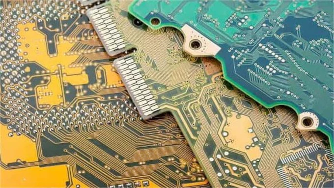
Laminated Structure of Multilayer PCBs Lead-free HASL (Hot Air Solder Leveling) and ENIG (Electroless Nickel Immersion Gold) are two common PCB surface finishes. Lead-free HASL offers good solderability