
Home > PCB Assembly
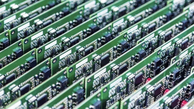
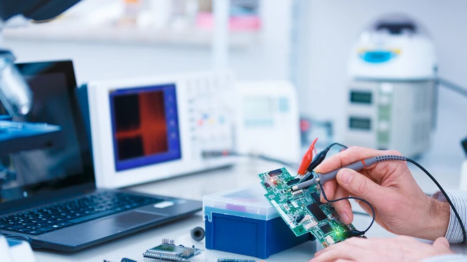
Expert PCB Assembly Services in China – Quality, Speed, and Reliability You Can Trust.
Our value-added services are designed to enhance your experience and provide additional benefits beyond our core offerings. From quality guarantees to personalized support, we are committed to going the extra mile to ensure your complete satisfaction.
Free DFM analysis to Ensure the PCB design is optimized for assembly, reducing errors and improving yield rates.
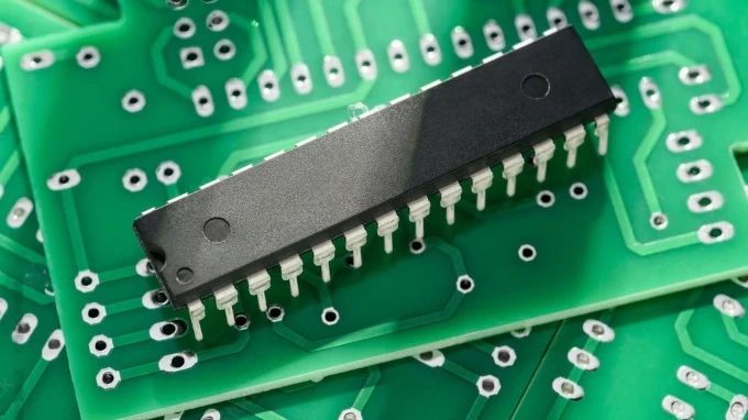
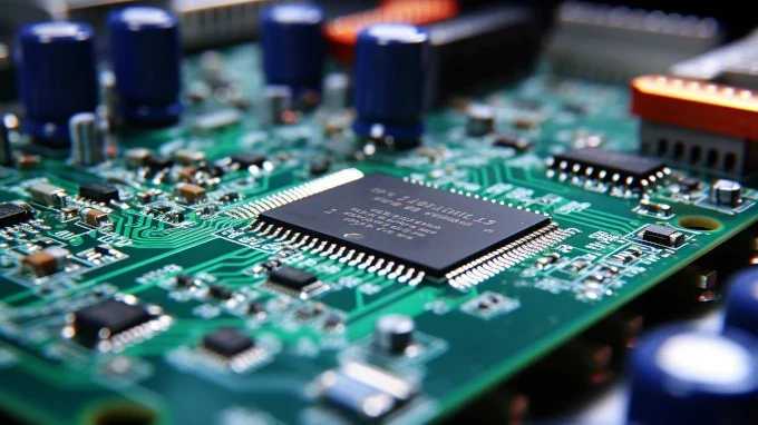
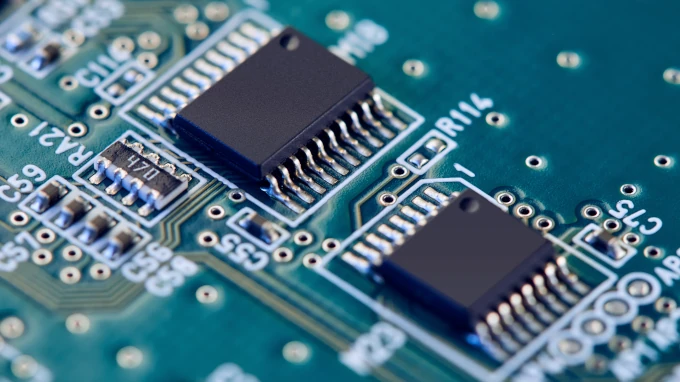
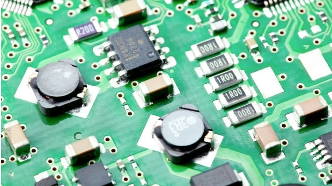
Support both Surface Mount Technology (SMT) and Through-Hole Technology (THT) for complex or hybrid PCB designs.
Expedited assembly services to meet tight deadlines, ideal for prototyping or urgent production needs.
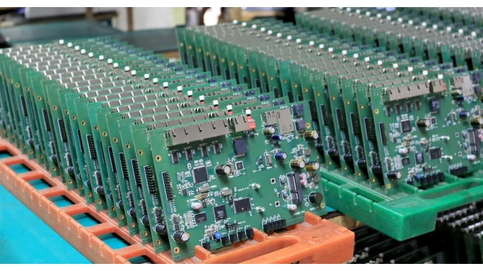
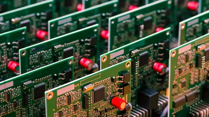
Comprehensive end-to-end service covering PCB fabrication, component sourcing, assembly, and testing, providing a seamless experience for customers.
| No. | Item | Feature | Standard | Advanced |
|---|---|---|---|---|
| 1 | Layer Count | Min~Max | 1~16L | 48 L(Max.) |
| 2 | Material | Types | FR-4, Aluminum/ Copper-base, Rogers | FR-4(Halogen-free), Arlon |
| 3 | Panel Size | Max | 508 x 610 mm(20”x 24”) | 508 x 1500 mm(20” x 34”) |
| 4 | Finished Thickness | Min~max | 0.2~5.0mm(0.005~0.126”) | 0.2~6.5mm(0.005~0.165”) |
| 5 | Trace Width/ Space | Inner/ Outer layer | 3/3mils(0.075/0.075mm) | 2/2mils(0.05/0.05mm) |
| 6 | Mechanical Drilling | Min | 0.008”(0.20mm) | 0.006”(0.15mm) |
| 7 | Mechanical Drilling | Max | 0.197”(5.0mm) | 0.256”(6.5mm) |
| 8 | Laser Drilling | Min | 0.006”(0.15mm) | 0.004”(0.10mm) |
| 9 | Aspect Ratio | Max | 12:1 | 20:1 |
| 10 | Copper Thickness | Min~max | 0.5~6 OZ | 20 OZ(max) |
| 11 | Solder Mask | Color | Glossy/Matt Green, white, black, red, blue | Yellow, pink, purple |
| 12 | Silkscreen | Color | White, black | / |
| 13 | Surface Finish | Types | HASL, Immersion Gold/ Tin/ Silver, Plating hard Gold, OSP | ENEPIG |
| 14 | Routing | Bit diameter | 0.093”, 0.062”, 0.031” | 0.021” |
| 15 | Profile | Tolerance | ±0.006”(0.15mm) | ±0.004”(0.10mm) |
| 16 | V-scoring | Angle | 30° | 20°/ 45°/ 60° |
| 17 | Plating Hard Gold | Thickness | 0.032”(0.8um) typical | 0.050”(max) |
| 18 | Special Processes | / | Carbon Ink, Peelable Mask, depth controll milling | / |
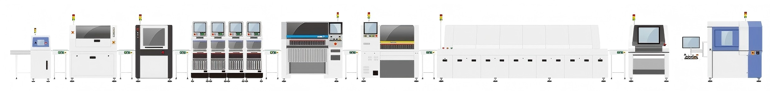
| PCB Loader | Solder Paste Printing | 3D SPI | Fuji NXT III | Fuji AIMEX III | Fuji XPF | Reflow Oven | AOI | 3D X-Ray |
|---|---|---|---|---|---|---|---|---|
| The first automated step, where boards are fed into the assembly line, ensuring consistent orientation and spacing for downstream processes. | High precision high stability solder paste printing, Printing accuracy ±0.025mm, Screen frame size: 470*380-900*900mm, PCB size: 50*50 ~ 600*610mm PCB thickness: 0.4-5mm. | 3D white light PSLM PMP, Bad detection types: missing printing, less tin, more tin, even tin, deviation, bad shape, surface pollution Maximum PCB size: 510 x 505mm. | Fuji latest generation of high-speed mounting modules. Single module component mounting capacity up to 37500CPH. Can mount 01005, 0201, 0402 and other devices. Can mount the next generation of 03015 ultra-precision devices. | Minimum mouting package: 03015, Number of stickers: 35000CPH, PCB size: 48*48mm-774*710mm, Chip precision: minimum ±0.034mm, IC chip precision: ±0.025mm. | Minimum mouting package: 01005, Chip/0.35mm BGA, PCB thickness: 0.3-6.5mm, PCB size: 50*50mm ~ 686 x 508mm, Chip precision: minimum ±0.04mm, IC chip precision: ±0.03mm. | 12 temperature heating zones, Heating time: around 30 minutes, PCB temperature distribution deviation: < 1.5℃, Maximum width of PCB: 610mm. | PCB size: 630 x 520mm, PCB thickness: 0.5 ~ 5.0mm, PCB component height: upper:35mm, lower: 110mm, PCB warping degree: bending less than 3mm is acceptable. | Maximum sample size: 800 x 500mm, Number of PCT production photos: 360, Number of photos produced by ACT:1500-1800, Resolution: 0.75um minimum. |
The PCB assembly process is a systematic sequence that transforms a bare PCB into a functional electronic device. It involves multiple stages utilizing specialized equipment and quality controls, ensuring reliable and efficient integration of components according to design specifications.
Verify all customer-provided data (Gerber, BOM, pick-and-place, drawings) as well as the bare PCBs to ensure manufacturability, functionality, reliability, and cost-effectiveness. Raise EQ if needed and prepare MI for production.
Bake bare PCBs and moisture-sensitive components (ICs, BGAs, plastic packages) to remove moisture and prevent soldering defects such as popcorning or delamination.
Transfer bare PCBs smoothly into the SMT production line using automatic loaders, conveyors, and buffers to ensure stable handling and consistent flow before solder paste printing.
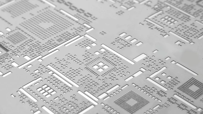
Apply solder paste onto PCB pads using a stainless-steel stencil to ensure accurate deposition for SMT component mounting.
Use 3D SPI equipment to check solder paste volume, height, and alignment before placement to avoid bridging and insufficient solder joints.
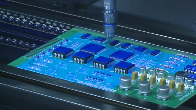
High-speed placement machines accurately mount surface-mount components onto the PCB according to the placement program.
Boards pass through a reflow oven where solder paste melts and solidifies, forming reliable electrical and mechanical joints for all SMT components.
Optical inspection detects missing components, polarity errors, tombstoning, bridging, and other defects after reflow.
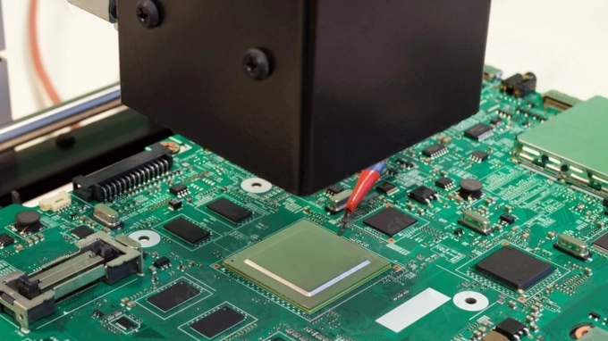
Non-destructive X-ray imaging checks hidden solder joints under BGAs, LGAs, QFNs, and other bottom-terminated components.
Manually or automatically insert through-hole components such as connectors, large capacitors, transformers, and mechanical parts.
Solder all THT leads using wave soldering or precision selective soldering for mixed-technology assemblies.
Skilled technicians perform manual soldering for special, oversized, or sensitive components where automation is not suitable.
Remove flux residues, contaminants, and ionic materials to prevent corrosion and ensure long-term reliability, especially for high-reliability products.
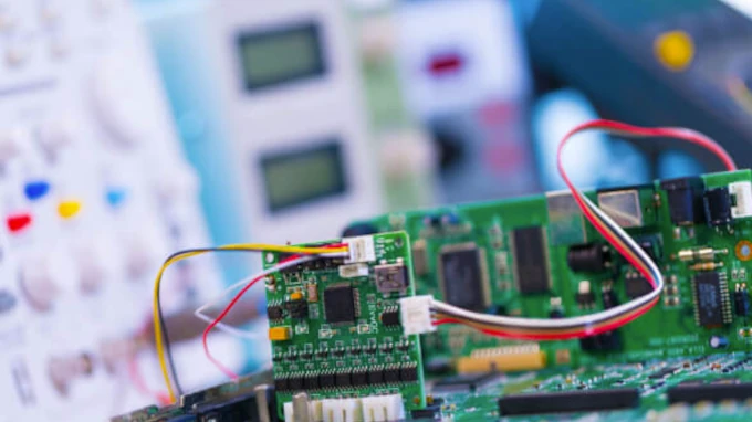
Perform tests such as In-Circuit Test, Flying Probe, and Functional Circuit Test to verify electrical performance and system functionality.
Apply protective coating to shield PCBs from moisture, dust, chemicals, and temperature cycling—used in automotive, aerospace, outdoor, and industrial applications.
Separate individual PCB units from the manufacturing panel using methods such as V-cut, routing, laser cutting, or punching, ensuring clean edges and preventing stress or damage to components.
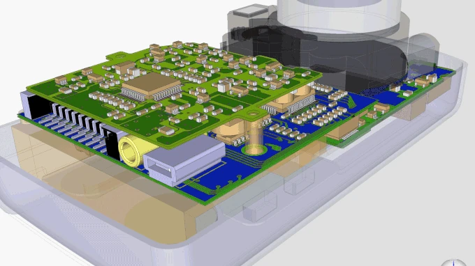
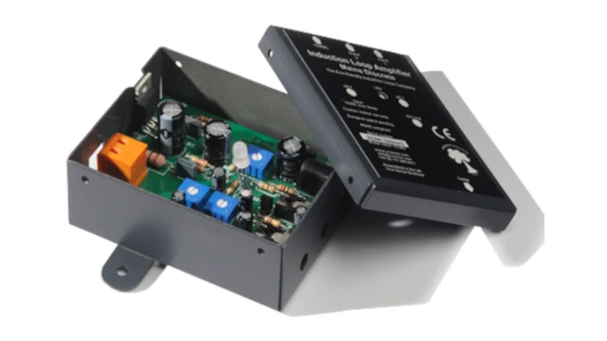
Assemble PCBs into enclosures, add cables, display modules, heatsinks, mechanical parts, and perform full system integration.
Run boards under load and elevated temperature to detect early-life failures and ensure long-term stability.
Perform visual, mechanical, and electrical checks to confirm product meets specifications, standards, and customer requirements.
Use ESD-safe packaging, labeling, and moisture protection. Ship finished assemblies according to customer logistics instructions.
In-depth and comprehensive overview of PCB industry standards and best practices required for ensuring quality assurance and consistency across all production processes.