Backplane PCB

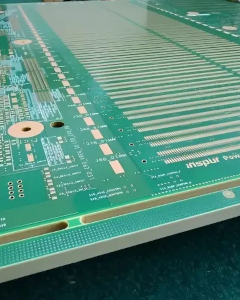
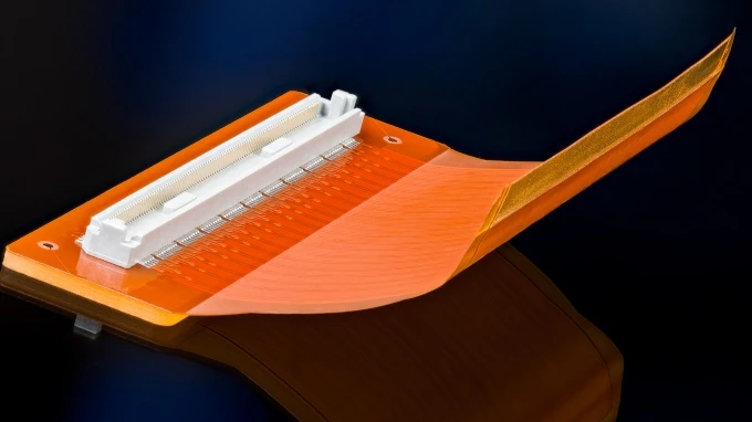
Backplane PCBs are specialized multilayer boards featuring numerous connectors for daughter cards, typically press-fit rather than soldered, which reduces exposure to high soldering temperatures. This design allows for increased thickness without concerns over z-axis expansion. Commonly found in large routers and switches that support Internet backbones and server farms, these PCBs handle high data path bandwidth, reaching speeds of up to 28 Gb/s. However, the parasitic capacitance of plated through holes can impact performance, leading to techniques like back drilling to optimize their fabrication.

Backplane PCB Key Features

Backplane PCBs include high layer counts to support dense interconnections, robust mechanical strength for supporting multiple plug-in cards, controlled impedance for high-speed signal transmission, and optimized material selection to reduce signal loss and crosstalk. They are also designed for high reliability, excellent thermal management, and ease of maintenance or upgrades in large electronic assemblies such as data centers and telecommunications infrastructure.

Backplane PCBs require a careful balance of electrical, mechanical, and thermal design considerations to support complex systems and maintain system reliability, often customized per application.

What is a backplane PCB?

A backplane PCB is a large, multilayer circuit board that serves as a backbone for interconnecting multiple daughter boards or plug-in cards. It provides both power distribution and high-speed signal routing.

They allow large numbers of high-speed connections (often 25–112 Gbps per lane) between multiple boards, maintaining signal integrity while minimizing cabling and complexity.

Challenges include managing very high layer counts (20–60+), routing dense differential pairs, controlling impedance across long traces, and minimizing stub effects with back-drilling.

High-performance laminates such as Panasonic Megtron, Isola Tachyon, or Nelco SI materials are chosen for their low dielectric loss (Df) and stable dielectric constant (Dk) at high frequencies.

The process involves sequential lamination of multiple core and prepreg layers, deep-hole drilling, copper plating, back-drilling for signal integrity, and strict alignment using X-ray drilling systems.

How are connectors mounted on backplane PCBs?

Connectors are often press-fit for mechanical robustness and signal reliability, though soldered and hybrid approaches are also used depending on application.

Electrical tests verify thousands of connections, TDR measures impedance accuracy, cross-sectioning checks plating thickness, and reliability testing includes vibration, thermal cycling, and mechanical stress tests.

Yes. The cost is higher due to extreme thickness, high layer counts, specialized laminates, deep drilling, and the complexity of plating and lamination processes.

Telecom (5G base stations, routers), data centers (server racks, storage systems), aerospace, military systems, transportation, and large industrial automation equipment.

IPC-6012 (rigid PCB qualification), IPC-6018 (RF/high-frequency boards), and IPC-2221/2222 (generic design standards) are applied, often with customer-specific telecom and defense reliability standards.

FAQs

Common FAQ topics. If you have specific questions in mind, feel free to ask!

Related Products