Heavy Copper PCB

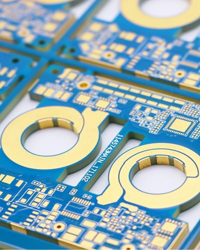
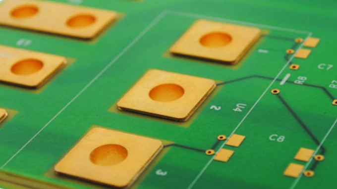
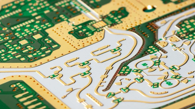
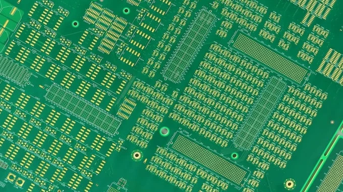
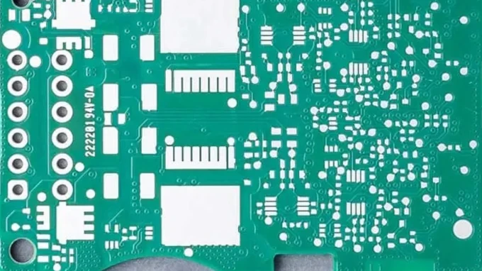
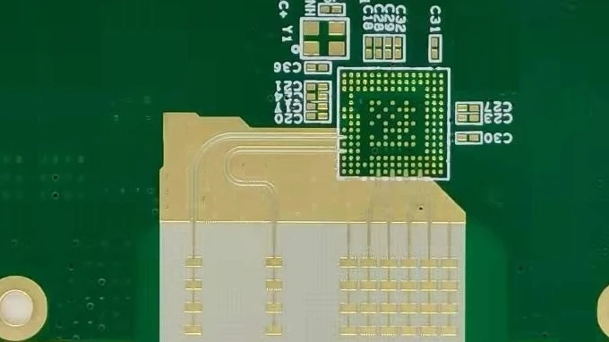
Heavy(thick) Copper PCB is compared with standard copper weight PCB, standard PCB copper thickness is always 0.5 ounce(oz) or 1 oz(35 micrometers or 1.4mil) per square foot, or even 2/2 oz. While heavy copper PCB generally have a copper thickness that exceeds 3 oz(105 micrometers), and can go up to 20 oz or even more. Heavy copper PCBs are commonly used in power electronics, such as high-power amplifiers, power converters, power distributors, welding equipment, radiators, planar transformers and motor controllers etc. They are also used in applications that require high reliability and durability, such as aerospace, military, and medical equipment. The heavy copper layers can provide better thermal dissipation, improved mechanical strength, and better resistance to corrosion and wear.

Heavy Copper PCB Summary

Heavy Copper PCBs are printed circuit boards that incorporate significantly thicker copper layers than standard PCBs, typically exceeding 3 oz per square foot (approximately 105 µm thickness) and sometimes going up to 20 oz or more. These boards are designed to handle high current loads and provide enhanced thermal management. Below are the key characteristics of heavy copper PCBs.

1. Thick Copper Layers

Heavy copper layers increase the current carrying capacity, reduce resistive losses, and improve heat dissipation.

Commonly used in power electronics, automotive, aerospace, and industrial equipment where high current capacity and heat management are critical.

Increased copper thickness requires special processes for etching, plating, and thermal treatment. Controlling dimensional stability and preventing warpage are important.

Heavy copper enables effective conduction of heat away from hot components, contributing to improved reliability.

Additional copper thickness also enhances the mechanical robustness of PCBs, supporting heavier components and connectors.

HDI laminates conform to standards such as IPC-4104 and IPC/JPCA-4104, which specify classification, conformance, and quality assurance for materials intended for high-density interconnect applications.

FAQs

Common FAQ topics. If you have specific questions in mind, feel free to ask!

What is considered a heavy copper PCB?

A heavy copper PCB typically has copper thickness starting at 3 oz (105 µm) per layer, going up to 20 oz (700 µm) or even higher in extreme cases. These boards are designed for applications that require high current handling, thermal management, and durability beyond what standard PCBs can provide.

Heavy copper PCBs carry larger currents without overheating, thanks to their high copper mass and improved thermal conductivity. This makes them ideal for power converters, motor controllers, automotive battery systems, and high-current switching devices.

Designers should use wider traces, larger pads, and increased spacing to prevent shorts during etching and soldering. Thermal relief patterns may be added to balance heat flow, and dielectric thicknesses must be optimized for both electrical isolation and mechanical strength.

Yes. Processes like differential etching, pulse plating, and sequential lamination are commonly used. These help maintain copper thickness uniformity while avoiding over-etching and resin starvation in thick copper areas.

IPC-2221 (generic design standards), IPC-6012 (qualification and performance specifications), and IPC-A-600 (acceptability of boards) set the quality benchmarks for copper thickness, plating adhesion, and electrical performance in heavy copper PCBs.

How does heavy copper affect soldering and assembly?

Thick copper layers absorb more heat, so standard soldering profiles may not achieve proper wetting. Controlled reflow temperatures, pre-heating stages, and high-performance solder alloys ensure proper bonding without damaging the board or components.

In addition to E-testing for continuity, thermal shock tests simulate real-world temperature cycles. Cross-sectional micrographs verify copper thickness and adhesion, while X-ray inspection checks internal solder joints in high-current components.

Yes. Costs rise due to thicker copper foils, longer plating times, advanced lamination processes, and lower production yields. However, they reduce the need for additional heat sinks or mechanical reinforcements, offsetting some expenses in high-power designs.

Heavy copper PCBs are essential in automotive electronics (EV powertrains, charging stations), renewable energy (solar inverters, wind power converters), industrial automation (motor drivers, robotics), and aerospace defense electronics for reliability under harsh conditions.

While most heavy copper PCBs range from 3 oz to 10 oz per layer, ultra-heavy designs can reach 20 oz or even higher. These are used in specialized applications like welding equipment, military radar systems, and large-scale power distribution units.

Related Products