Home > PCB Fabrication > MiniLED PCB
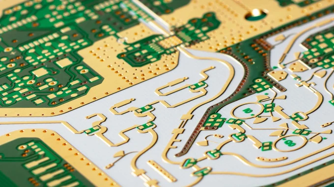
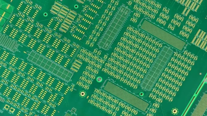
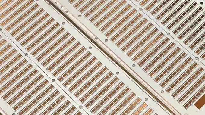
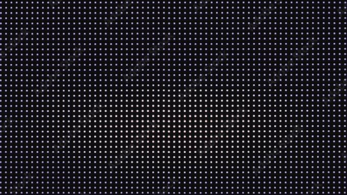
A MiniLED PCB is a specialized printed circuit board designed to support MiniLED chips, which are extremely small packaged LEDs—typically 100–300 μm in size. Compared with traditional LEDs, MiniLEDs allow higher brightness, better contrast, finer pixel pitch, and lower power consumption, making them ideal for next-generation display technologies.
MiniLED PCBs must meet stricter thermal, dimensional, and optical control requirements because thousands to tens of thousands of LED chips are mounted on a single board.
Essential information includes part numbers, fabrication and drill drawings, manufacturing notes, board details, material specifications, conductor patterns, artwork data for both sides, aperture lists, drill data, netlist data, and any special requirements.
Designers focus on layer count optimization, power/ground plane placement, controlled impedance routing, signal isolation, thermal dissipation, and via structures (blind, buried, or through-hole) for reliable connectivity.
Typical layer counts are 4 to 8 layers, common for consumer electronics and networking and telecom devices.
Typical materials include prepreg (pre-impregnated dielectric sheets), core substrates made from fiberglass-reinforced laminates like FR-4 or specialized materials for high-speed/high-frequency applications, and copper foils. Advanced multilayer PCBs may also use high-speed dielectric substrates like Rogers or PTFE-based materials for specific electrical properties.
Proper layer stacking, controlled impedance routing, and short signal path design help minimize signal reflections, crosstalk, and electromagnetic interference. Careful via placement and ground plane design are critical for maintaining high-speed signal quality and reducing noise.
Higher component density (saves space), improved signal integrity (reduced EMI and crosstalk), better power distribution (dedicated power and ground planes), enhanced durability (rigid structure).
Number of layers (more layers = higher cost), material selection (high-frequency or exotic materials cost more), Via types (blind/buried vias increase cost), tolerances & testing (tight specs require more QA).
Consumer electronics, telecom equipment, aerospace avionics, medical imaging devices, automotive radar systems, and industrial automation heavily rely on multilayer PCB technology.
Electrical testing detects opens/shorts, AOI checks for surface defects, microsection analysis verifies inner-layer integrity, and X-ray inspection ensures proper via filling and solder joint quality.
High layer counts increase board thickness and thermal mass, making reflow soldering more complex. Warpage, fine-pitch BGA soldering, and mixed SMT/through-hole components also require precise assembly techniques.
Common FAQ topics. If you have specific questions in mind, feel free to ask!