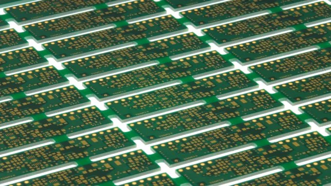
Double-sided PCB is a type of circuit board that offers a ground, between the simplicity of single sided PCBs and the complexity of multilayer PCBs. Double sided PCB has conductive copper on both sides allowing for more intricate and denser traces compared to single sided PCBs.
This structure offers advantages. Firstly it enables the creation of circuits without significantly increasing the size of the board, which makes it perfect for compact electronic devices. Additionally, it has two sides of conductive layers means that components can be placed on both sides enhancing functionality within a given area.
To connect components on both sides small holes called vias are drilled on the board. These vias are then plated through with copper (or filled by conductive materials as Silver-through holes), creating electrical connections between the two layers. This technique allows designers to design circuits that could not be possible with single-sided PCBs.
Double-sided PCBs are widely used in various electronic applications like consumer electronics, industrial controls, power supplies, converters and more. They strike a balance between the simplicity and cost effectiveness of single-sided PCBs and the high density and functionality of multilayer PCBs.
Double-Sided PCB Manufacturing
High quality 2 Layer PCB manufacturing beyond your expectation in our modern facility.

State-Of-The-Art Equipment
- Laser Direct Imaging for Patterns.
- VCP(Vertical Continuous Copper Plating) line.
- Laser Direct Imaging for solder mask.
- AVI(Automated Visual Inspection).
- All surface finishes in house excluding ENEPIG.
Extensive Services We Offer
- Prototype PCB Quickturn as fast as 24 hours.
- Small to medium volume PCB Quickturn as fast as 5~7 wds.
- 100% online AOI, X-ray, 100% E-testing.
- Additional services: Components sourcing, PCB Assembly.

