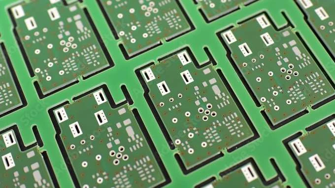
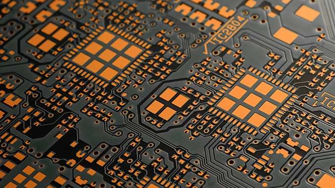
Multilayer PCB consists of three or more conductive copper layers separated by insulating dielectric, usually even layers such as 4, 6, 8 layer etc. Main applications of multialyer PCBs used to be confined to sophisticated industrial electronic products. However nowadays, they are the mainstream of most electronic devices. The layers are bonded together with heat and adhesive to create a single, integrated board. The inner layers are made of substrate material known as the core, and the insulating layers are often referred to as prepreg. Prepreg is a glass-reinforced epoxy material impregnated with resin, and it facilitates the bonding of copper layers.
The inner layers may be a combination of various signal layers and ground & power planes used to distribute power to the components mounted on the outside layers. Connections are made between the outer layers and the inner layers with plated through holes(PTH) and vias. Multilayer PCB introduces the lamination process, which is where we actually creates the composite PCB from layers of circuitry in a lamination press under high pressure and heat. After pressing, multilayer PCBs manufacturing processes are almost the same as a traditional double-sided PCBs.
High Quality Multilayer PCB Manufacturing
Union Circuits employs cutting-edge manufacturing processes for its multilayer PCBs. This involves advanced techniques in material selection, lamination, exposure, etching, plating etc, ensuring that each PCB meets the highest standards of quality and reliability.
State-Of-The-Art Equipment
- Cedal Laminator in house which is essential for mulitlayer PCB manufacturing.
- Laser Direct Imaging for Patterns.
- VCP(Vertical Continuous Copper Plating) line.
- Laser Direct Imaging for solder mask.
- AVI(Automated Visual Inspection).
- All surface finishes in house excluding ENEPIG.
Extensive Services We Offer
- Prototype PCB Quickturn as fast as 24 hours.
- Small to medium volume PCB Quickturn as fast as 5~7 wds.
- 100% online AOI, X-ray, 100% E-testing.
- Additional services: Components sourcing, PCB Assembly.