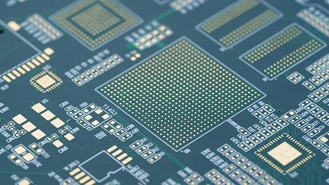
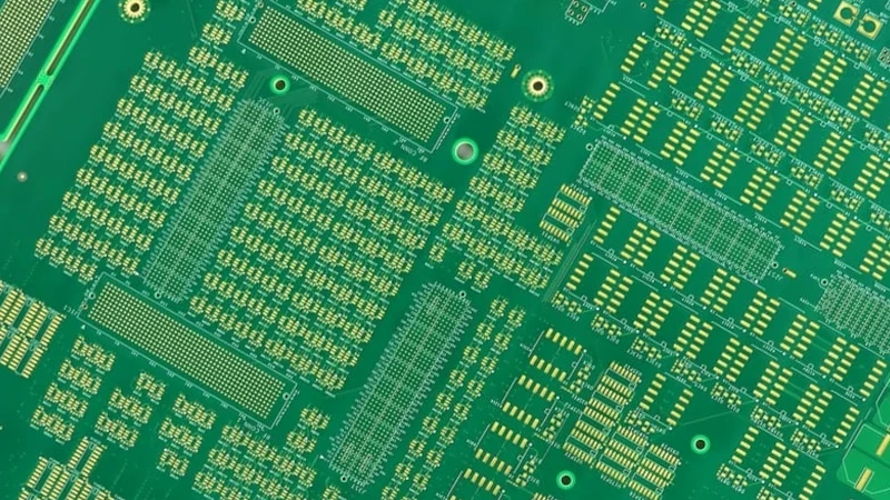
High Density Interconnect (HDI) PCBs are advanced circuit boards characterized by a higher line density than traditional PCBs. They employ micro blind and buried via technologies, essential for meeting the electrical demands of high-speed signals. The development of these boards is driven by the need for impedance control with alternating current characteristics, high-frequency transmission, and minimizing electromagnetic interference (EMI). Utilizing Stripline and Microstrip structures, HDI PCBs often feature multi-layer designs.
These boards use insulating materials with low dielectric constants and attenuation rates to enhance signal transmission quality. To accommodate the miniaturization and dense arrangement of electronic components, HDI PCBs incorporate sophisticated features like laser blind vias, mechanical buried vias, stacked and staggered vias, and fine lines with small gaps. Microvia holes, typically 4mil & 6mil in diameter made by laser drilling, connect the inner and outer layers.
The increasing complexity of components with high input/output counts has led to the development of new fabrication techniques. These include laser drilling, micro-punching, mass etching, photosensitive dielectric materials for dielectric creation, and innovative metallizing methods like conductive adhesives. These advancements enable higher routing density, size and weight reduction, and improved electrical performance.
HDI PCBs are essential in numerous applications, such as smartphones, tablets, laptops, wearable devices, and automotive electronics etc. Their ability to integrate complex functionalities into a compact design significantly contributes to the miniaturization and advancement of electronic devices.
High Quality HDI PCB Manufacturing
Union Circuits employs cutting-edge manufacturing processes for its HDI PCB Manufacturing. This involves advanced techniques in material selection, lamination, exposure, etching, plating etc, ensuring that each PCB meets the highest standards of quality and reliability.

Key Equipment
- Laser drilling for HDI PCB manufacturing, microvia types: stacked/staggered; via size: 4mil & 6mil; via filling: conductive epoxy or electrodeposited copper
- Laser Direct Imaging for Patterning, high imaging quality and high throughput for applications such as advanced multilayer boards, HDI, flex.
- Laser Direct Imaging for solder mask.
- AVI(Automated Visual Inspection).
- All surface finishes in house excluding ENEPIG.
Extensive Services We Offer
- Quick turnaround HDI Prototypes as quick as 5 working days.
- Small to medium HDI PCB production.
- 100% online AOI, X-ray, 100% E-testing.
- Additional services: Components sourcing, PCB Assembly.

