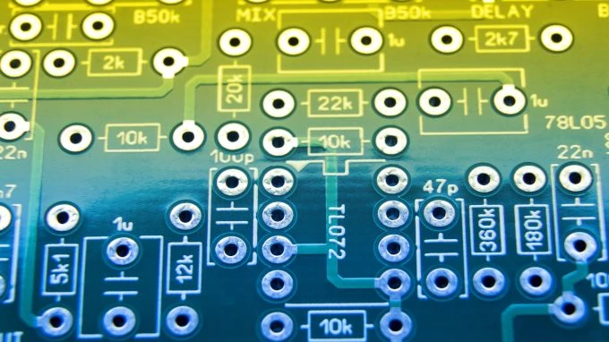
Single-sided PCBs, also known as print-and-etch boards, are boards with traces on only one side. The etch resist is typically applied using screen printing techniques, and the conductor pattern is formed by chemically etching away the unwanted copper foil that is exposed. These are traditional single-sided PCBs, common used materials are FR-1, CEM-1, CEM-3, and FR-4. Of course there are some other types of boards also single-sided, like the flexible circuits and metal core PCBs, a lot of them also in single-sided, the processes are different and much more complex.
Typical Materials
Single-sided PCBs offer use low-cost and relatively low functionality materials, always in high-volume. Here are a few common used materials.
- FR-1-- a paper-based material, FR-1 is economical but has limitations in terms of heat resistance.
- CEM-1-- composite Epoxy Material (CEM-1) is a step up from FR-1, offering better heat resistance and strength.
- CEM-3 -- similar to FR-4 in many aspects, CEM-3 is white, which makes it preferable for LED applications.
- FR-4 -- the industry standard FR-4, is known for its excellent electrical insulation and heat resistance, suitable for a wide array of applications, cost relatively higher than all above.
Fabrication Process
Given the emphasis on cost and low complexity, single-sided boards are generally produced in highly automated, conveyorized print-and-etch lines, using the following basic process flow.
- Material cutting: cut substrate into appropriate panel size.
- Loading: place panelsin loader which feeds them into the line.
- Panel cleaning.
- Printingultraviolet curable etch-resist ink.
- Cure the etch-resist ink.
- Exposed copperetching.
- Striping: strip the resist.
- Applyingsolder resist.
- Legendprinting.
- Drilling(glass-based substrate)or punching(paper-based substrate) the holes.
- E-testing: test for shorts and opens.

Process Variations
In some variations, the conductor surface of the PWB gets insulated, exposing only pads, and then conductive paste is screened to form additional conductors on the same side of the board, thus forming double conductive layers on a single side. Most metal-core PWB consumer applications are made of aluminum substrate, which comes as a copper-clad material. PWBs made of such material do not have through-holes, and components are usually surface-mount types. These circuits are frequently formed into three-dimensional shapes.
