
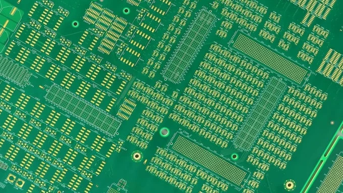
HDI PCB Key Features High-Density Interconnect (HDI) PCBs are advanced circuit boards designed for complex, high-density electronic assemblies. The key features of HDI PCBs include: 1. Microvias and Laser Drilling HDI PCBs utilize microvias—small-diameter vias typically drilled with laser technology—to create interlayer connections. These microvias are often only a few mils in diameter and allow for high interconnection density while preserving space for routing. 2. Blind and Buried Vias HDI technology incorporates blind vias (connecting outer layers to internal layers without passing through the entire PCB) and buried vias (restricted to internal layers), which enable more routing channels and reduce via count
Lead-free HASL (Hot Air Solder Leveling) and ENIG (Electroless Nickel Immersion Gold) are two common PCB surface finishes. Lead-free HASL offers good solderability and is cost-effective but can result in uneven surfaces and is less suitable for fine-pitch components. ENIG, on the other hand, provides a very flat surface, excellent for fine-pitch and BGA components, along with superior corrosion resistance and long shelf life, though it is more expensive. Choice between them depends on application requirements for reliability, planarity, and cost. Lead-free HASL Lead-free HASL (Hot Air Solder Leveling) is a surface finish process used in the manufacturing of printed circuit boards
Reflow soldering temperature setting is a precise and critical process in electronics manufacturing, as it determines the quality and reliability of solder joints by carefully controlling the heating and cooling of circuit boards during assembly. Proper temperature profiling ensures effective solder flow, minimizes thermal stress on components, and leads to robust connections, all of which are crucial for the long-term performance and durability of electronic devices. 1. Preheat Stage In the preheat stage, the assembled circuit board is gradually heated from room temperature to a moderate level. The primary purpose is to gently warm the components and the PCB, preventing thermal shock
Lead-free HASL (Hot Air Solder Leveling) and ENIG (Electroless Nickel Immersion Gold) are two common PCB surface finishes. Lead-free HASL offers good solderability and is cost-effective but can result in uneven surfaces and is less suitable for fine-pitch components. ENIG, on the other hand, provides a very flat surface, excellent for fine-pitch and BGA components, along with superior corrosion resistance and long shelf life, though it is more expensive. Choice between them depends on application requirements for reliability, planarity, and cost. Lead-free HASL Lead-free HASL (Hot Air Solder Leveling) is a surface finish process used in the manufacturing of printed circuit boards
Electronic component packages such as 01005, 0201, 0402, 0603, 0805, and 1206 refer to standardized surface-mount device (SMD) sizes, each defined by their physical dimensions in both inches and millimeters. These codes are widely used for resistors, capacitors, and other SMD components, and choosing the right size is important for compatibility, space management, and circuit performance. Typical SMD package sizes 01005: This is one of the smallest available packages, measuring 0.01 inches × 0.005 inches (0.4 mm × 0.2 mm). Its ultra-miniature size makes it suitable for highly compact devices like smartphones and modern wearables. 0201: At 0.02 inches × 0.01 inches